
 English
 usheenthermal

Thermal Pad Selection for AP and BMS Assemblies
Date:2026-10-21
Most thermal pad guides read like a menu: pick a conductivity, pick a thickness, done. Real assemblies are less cooperative. Gap, compression ratio, contact thermal resistance, and assembly stress all occupy the same interface. They negotiate with one another whether the spreadsheet has a column for it or not.
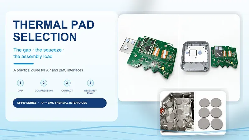
Here is the practical version:
- The thickness works only if it makes solid contact at both ends of the tolerance stack.
- The thermal result counts only if you verify it at the actual compressed state, not just the catalog condition.
- The sample is ready for production only after thickness tolerance, supply configuration, and incoming inspection are settled.
To make that judgment concrete, let us walk through the AP, control-board, and power-module interfaces described in the source material.
One Heatsink Two Problems
Here is a scene that will feel familiar. One heatsink plate has to couple to several heat sources at once. During prototyping, one device runs hot, so the team thickens the pad and sees the temperature improve. Then another location shows a deep imprint, or assembly starts reporting higher load. The same fix has created a second problem.
Cranking up thermal conductivity may sound like the obvious next move. But if the geometry is still wrong, that is mostly a more expensive way to keep the same structural contradiction.
Sheen's selection logic anchors on two positions at the same time:
- Solid contact at the largest gap.
- Controlled load at the smallest gap.
Get both ends right and the middle has a much better chance of behaving. The SF600 series is already used in volume at these kinds of interfaces, including inside and outside AP shield cans and on the backside of PA chips. These structures are useful proving grounds because thickness, conformity, and device stress have to be evaluated as a package deal.
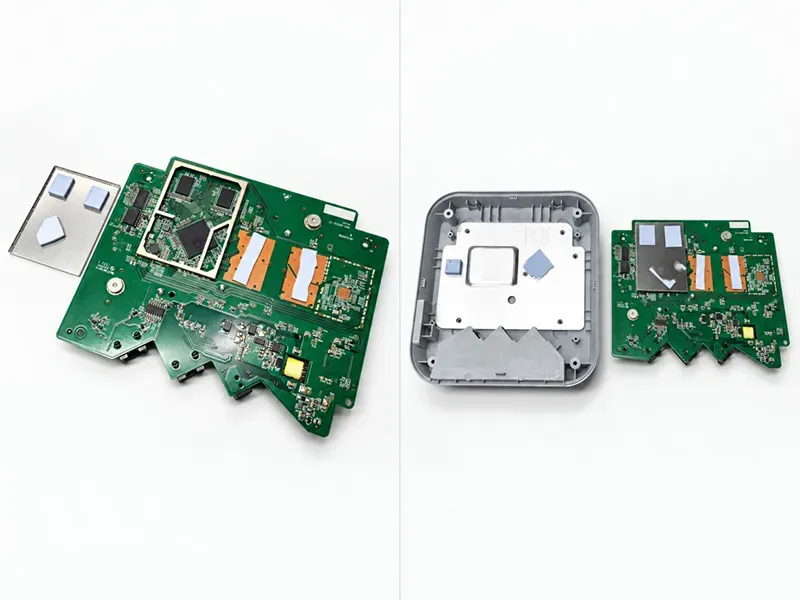
Figure 1. AP teardown example. The left view shows the sheet inside the shield; the right view shows the heatsink and board-side contact positions. The source material identifies the interfacial thermal material as Sheen SF600.
Step One Do the Gap Math All of It
A surprising number of 'the pad is not cooling well' mysteries trace back to a gap that was never fully computed. Start from a common assembly datum:
Gap = heatsink surface height relative to the PCB - device top height +/- relevant dimensional tolerances
Then add the parts that make real hardware less tidy: flatness, board warpage, and deformation after the fasteners are torqued. If thermal expansion changes the dimensions in a meaningful way, check the hot state too. One static caliper reading is a snapshot, not the whole movie.
Worked example: suppose the assembly analysis lands at a 0.8-1.2 mm gap and the selected pad starts at 1.5 mm thick. Ideal geometric compression is 20%-46.7%.
That tells you how much deformation the material may need to absorb. It does not yet prove the pad will hug the surface across the whole range without overloading the device.
Now add a project constraint: compression must stay between 20% and 40%. Ignoring the pad's own thickness tolerance for a moment:
- The largest gap, 1.2 mm, demands a pad at least 1.50 mm thick (1.2 / 0.8).
- The smallest gap, 0.8 mm, demands a pad no thicker than approximately 1.33 mm (0.8 / 0.6).
No overlap. The ranges do not even shake hands. In plain English, one thickness cannot satisfy both ends. The options are to tighten the structural tolerances, use zoned thicknesses, or revisit the deformation and load the material and device can actually tolerate.
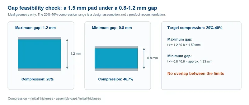
Figure 2. Gap feasibility check. This is an ideal geometric calculation, not a recommended compression range for any specific model.
And yes, the pad's own thickness tolerance belongs in the same spreadsheet. Two audit combinations catch most of the trouble:
- Maximum gap plus the thinnest incoming material checks for insufficient contact.
- Minimum gap plus the thickest incoming material checks for over-compression.
The wider the batch thickness spread, the thinner the design margin. Set the procurement tolerance at sample stage, not after the first bad lot arrives.
Step Two Pick the Actual Part Not the Series Brochure
For AP shield-can interfaces, SF600 is the natural starting conversation. For BMS interfaces, the documented direction is SF600D. Treat the model number as the front door, then go inside and confirm the specific hardness, thickness, and supply structure. A series performance range is a neighborhood, not a promise about every house in it.
Need a screening starting point? The published SF600G information lists thermal conductivity of 6.0 W/m·K under ASTM D5470, plus an area-normalized thermal resistance of 0.30 °C·in²/W at 1 mm and 30 psi. A Shore 00 hardness configuration is also listed.
| Property | Value | Condition or method |
|---|---|---|
| Thermal conductivity | 6.0 W/m·K | ASTM D5470 |
| Area-normalized thermal resistance | 0.30 °C·in²/W | 1 mm; 30 psi; ASTM D5470 |
| Standard hardness | Shore 00 40/60 +/- 5 | ASTM D2240; configuration to be confirmed |
| Thickness range | 0.5-5.0 mm | ASTM D374 |
Table 1. Selected published SF600G values. Use them as an inquiry starting point. Confirm the current model data and final configuration before ordering; do not extrapolate the thermal-resistance value to other thicknesses or pressures.
That gives the sample request a concrete target. It does not give you permission to extrapolate the same result to another thickness or lower installation pressure.
When contacting Sheen, state the objective plainly: the pad needs to conform within a defined gap, stay within the device-allowable load, and meet a verified thermal-resistance target at those conditions. For load-sensitive designs, ask for the pressure-compression curve for the specific formulation. Hardness is a first-pass filter, not a substitute for assembly-force judgment.
One more trap for multi-pad designs: when one heatsink plate sits on several pads, estimate the combined force from each location's pressed area and pressure. Then sanity-check the support and fastener layout. A single coupon that feels soft tells you very little about total plate load. The same pressure over a larger area is still more total force. Physics keeps the receipts.
Step Three Let the Assembly Tell You How to Test
The teardown view shows the inside of the shield can, the shield structure itself, and where the heatsink plate touches the board. Here is the catch with stacked interfaces: different positions can form series thermal paths. If one layer never gets properly compressed, changing another layer to a higher-conductivity material may buy you almost nothing.
During selection, record the gap and pad imprint layer by layer. Find the interface that is actually limiting the temperature rise.
For sample comparisons, hold the important variables constant:
- Power, ambient conditions, and airflow.
- Fastening method and measurement points.
- Post-assembly interface thickness, pad position, initial thickness, and batch.
Once the temperature is on target, inspect PCB warpage, device stress, and the contact state after teardown. Also remember: identical screw torque does not equal identical pad pressure. Torque travels through friction, fastener path, and structure stiffness before it becomes interface pressure. It is a commute with tolls.
Two special situations deserve their own line in the test plan:
- Silicone-sensitive requirements: discuss Sheen's AF non-silicone series separately. Check volatiles, migration, and temperature limits for the project. Do not copy-paste a silicone pad's structural recipe onto a non-silicone material and hope for the best.
- First-round samples: change one variable at a time. Compare candidate thicknesses within one model and configuration first; change thermal grades second. Match teardown imprint photos to temperature results so you can tell whether the improvement came from better conformity or from the material's thermal properties.
Step Four Bring Die Cutting and Supply Structure into Procurement
Sheen's material information lists one-sided or two-sided tack, reinforcement layers, and custom die cutting. For multi-position designs, discuss shapes and supply format by device zone and locating features. That is much closer to the real application than asking for a per-square-meter price and hoping the rest sorts itself out.
A few procurement ground rules:
- Any added tack layer or reinforcement changes the interface structure. Validate the final configuration, not just a bare-material coupon.
- Compare quotes on a level field: same grade, thickness, tolerance, dimensions, tack or adhesive, and packaging. Confirm lot traceability and change notification at the same time.
- For reworkable modules, dry-run release-liner handling, removal and cleanup, and material waste in a small-batch trial. 'The sample worked great' and 'mass production added labor' are both statements you do not want in the same report.
- Already running a competitor's part? Send the part number, thickness, and assembly method together. Check the technical deltas first, then discuss replacement validation and cost.
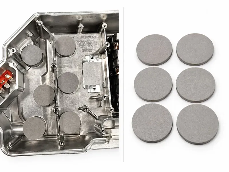
Figure 3. Circular pad shapes in a BMS structure. The supplied source identifies the SF600D application direction in the referenced presentation; final die-cut dimensions should be checked against the actual contact positions and assembly.
Bring Sheen One Interface Problem
If the project is fighting insufficient contact, rising force after thickening, or a higher-conductivity swap that did not move the temperature, start with three inputs: gap range, contact dimensions, and allowable load.
Load not defined yet? Describe the device package and the current assembly anomaly instead. That is enough to begin narrowing the candidate model, thickness, and supply configuration.
In one request, ask for:
- The current datasheet for the model in question.
- Samples at the target thickness.
- A custom die-cut quotation.
- Confirmation of which thermal-resistance and compression data apply to the target conditions.
【Request a Custom Quote】Anything the existing data does not cover becomes a validation-plan discussion. Bring the current material and target temperature too. That keeps the comparison anchored to your interface instead of drifting into a generic scorecard. The goal is not to win a catalog comparison. It is to find a thickness, formulation, and supply configuration that survives the actual assembly.
Technical data in this article is presented under the stated conditions. Confirm the current model data and final configuration before applying it to a production design.
Sheen Thermal
Dongguan Sheen Electronic Technology Co., Ltd · Founded in 2008
Manufacturer of thermal interface materials and silicone foam for automotive electronics, energy storage, power electronics, communications and consumer electronics.
Certified
- ISO 9001:2015
- ISO 14001:2015
- IATF 16949:2016
What we supply
- Thermal conductivity Up to 90 W/m·K
- Thickness 0.3–10.0 mm
- Custom & samples Die-cut to drawing, 3–7 days
LAST:Nothing