
 English
 usheenthermal

From Microscopic Contact to Lower Thermal Resistance: A Practical Guide to Sheen SP Phase-Change Materials
Date:2026-11-05
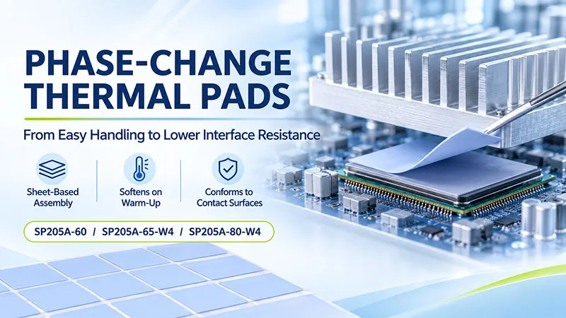
In servers, workstations, and compact electronics, the hardest part of cooling is sometimes hiding in plain sight: the thin interface between a chip and its heatsink. Two surfaces may look perfectly flat, yet microscopic roughness and trapped air still get in the way. Once the heatsink and airflow have been optimized, that little layer often becomes the next worthwhile place to look.
Sheen's SP phase-change materials combine easy room-temperature sheet handling with surface wetting after warm-up. You position a solid sheet during assembly. Then, when the interface reaches the grade's phase-change range under suitable pressure, the material softens and conforms to the contact surfaces. SP205A-60, SP205A-65-W4, and SP205A-80-W4 offer three candidates for projects that want low interface resistance without giving up a sheet-based assembly process.
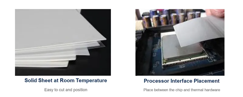
Figure 1. SP Series sheet form and processor-interface placement.
A High W/m·K Number Is Only Part of the Interface Story
Thermal conductivity describes how readily heat moves through the material itself. Interface resistance describes what happens in the assembled stack — and that is where material bulk resistance, contact on both sides, and final bond-line thickness all join the conversation. A larger W/m·K number, by itself, cannot tell you how the finished cooling structure will behave.
Phase-change materials are useful because they address both sides of that problem. Heating softens the material so it can wet the surfaces, while the allowed assembly pressure helps establish a conforming thermal interface. The same principle can apply to an air-cooled heatsink or a liquid cold plate. Whether it is the right route depends on contact area, interface temperature, flatness, and load — not on the product category alone.
What Changes When the Material Softens
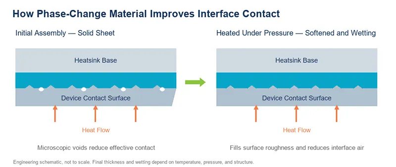
Figure 2. Interface contact before and after phase change. This mechanism schematic explains wetting and gap filling; it does not show actual thickness ratios or test results.
At room temperature, SP material remains a solid sheet with inherent tack to help hold its position. Compared with a paste that needs controlled dispensing shape and volume, a preform offers a drawing-based, place-and-clamp process. That makes it easier to standardize dimensions, coverage, and work instructions — fewer ‘who squeezed the tube today?’ variables.
Once the interface enters the selected grade's phase-change range and stays under suitable clamping conditions, the material softens, wets the surfaces, and fills microscopic peaks, valleys, and voids. Its job is to help heat keep moving into the heatsink. It is not a thermal battery that endlessly absorbs the device's operating heat through phase change.
Supplied Thickness Is Not Final BLT
Keep two thicknesses separate: the sheet's supplied thickness and the final bond-line thickness (BLT) after softening and compression. They are not interchangeable. You cannot simply insert nominal conductivity and supplied thickness into a formula and expect to reproduce a TDS thermal-resistance value. Final BLT and contact conditions need their own verification.
SP205A-60 vs SP205A-65-W4 vs SP205A-80-W4
| Property | SP205A-60 | SP205A-65-W4 | SP205A-80-W4 |
|---|---|---|---|
| Thermal conductivity, W/m·K | 6.0 ± 0.6 | 6.5 | 8.0 |
| TDS nominal thermal resistance, °C·in²/W | 0.015 | 0.010 | 0.007 |
| Same-value conversion, °C·cm²/W | ≈0.0968 | ≈0.0645 | ≈0.0452 |
| Stated resistance condition | 0.2 mm / 50 psi | 0.2 mm / 50 psi | 0.2 mm / 50 psi |
| Custom thickness, mm | 0.2–0.5 | 0.15–0.5 | 0.15–0.5 |
| Phase-change temperature, °C | 45–55 | 50–70 | 50–70 |
| Operating temperature, °C | −25 to 125 | −25 to 125 | −25 to 125 |
| Density, g/cm³ | 3.0 ± 0.3 | 2.7 | 2.8 |
| Color | Gray | Gray | Gray |
| Flammability listed in TDS | UL94 V-0 | Not listed | Not listed |
Table 1. Source: 20260117V0 TDS for all three grades. Conductivity and thermal resistance are marked ASTM D5470. 1 in² = 6.4516 cm²; the converted column is only a unit conversion of the same resistance values, not an additional test. 50 psi is approximately 345 kPa.
All three TDS documents mark RoHS, Halogen, and REACH as PASS, and list 200 × 300 mm sheets plus custom die-cutting. During product introduction, verify batch-specific compliance documents, die-cut drawings, and packaging requirements. A PASS marking on a material TDS is not a finished-equipment certification.
Use Nominal Resistance to Set the Test Order — Not the Final Winner
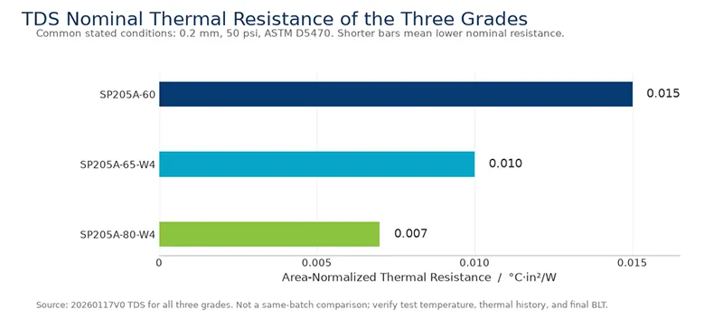
Figure 3. TDS nominal thermal resistance values side by side. Common stated conditions make initial screening easier, but this is not a head-to-head test with identical thermal histories and final BLTs.
Using the TDS values, SP205A-65-W4's nominal resistance is about 33.3% lower than SP205A-60's, and SP205A-80-W4's is about 53.3% lower. Those percentages describe differences between documents. They do not mean chip temperature will fall by the same percentage, and they certainly cannot be converted directly into system energy savings. Measure the actual improvement in the same structure and operating condition.
SP205A-60: Establish the Sheet-Process Baseline
For teams moving from paste dispensing to preforms, or establishing an assembly standard for phase-change material, SP205A-60 is a sensible baseline sample. It offers 6.0 ± 0.6 W/m·K conductivity and a nominal 0.015 °C·in²/W thermal resistance. First validate placement, coverage, compression, and post-run contact; then decide whether a lower-resistance W4 grade is worth the next step.
SP205A-65-W4: Push Interface Resistance Lower
When the same cooling structure needs a lower-resistance candidate, add SP205A-65-W4 to the comparison. It combines 6.5 W/m·K conductivity, nominal resistance of 0.010 °C·in²/W, and a custom thickness range of 0.15–0.5 mm. Focus the evaluation on resistance under actual pressure and phase-change conditions, plus assembly repeatability.
SP205A-80-W4: Start Here for a Tighter Resistance Budget
If the chip-to-heatsink resistance budget is tight and the lowest nominal value among these three is the first priority, start sampling with SP205A-80-W4. It offers 8.0 W/m·K conductivity and nominal resistance of 0.007 °C·in²/W. It deserves early testing, but the final choice still belongs to structural fit, reliability, yield, and purchasing conditions as much as to the datasheet.
Where SP Materials Fit
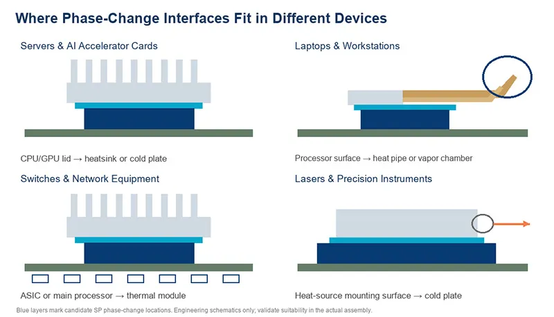
Figure 4. Candidate interface locations in four equipment categories. Blue layers indicate phase-change interfaces. These are engineering schematics, not customer cases or platform-specific compatibility certifications.
Server CPUs, GPUs and AI Accelerator Cards

Figure 5. Engineering illustration for server CPU and GPU applications. The interface layer is enlarged for visibility; actual selection requires validation.
For servers and AI accelerator cards, start with the external interface between the processor's metal lid and the heatsink or cold plate. Here, the material works together with contact area, surface flatness, and the clamping structure to move heat into the rest of the cooling system.
If the existing design has a tight interface-resistance budget, compare SP205A-80-W4 with SP205A-65-W4 and keep SP205A-60 as the baseline. Hold chip load, airflow, or coolant inlet conditions constant, then record steady-state temperature and contact condition. An external interface on a lidded device is not the same as TIM1 inside the package. Bare-die contact designs need separate verification of mechanical load and package compatibility.
Laptops, Mini PCs and Workstations
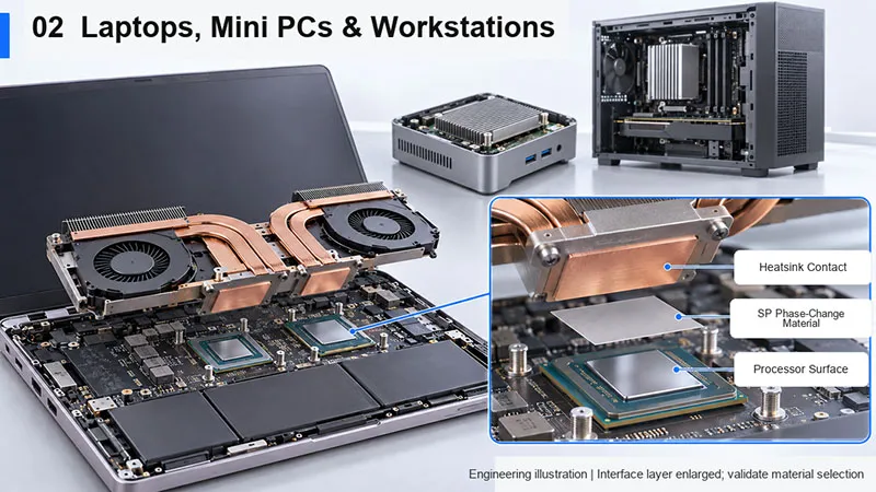
Figure 6. Engineering illustration for laptop applications. The interface layer is enlarged for visibility; actual selection requires validation.
These devices pack processors, heat pipes, vapor chambers, and fans into very little space. SP preforms can be evaluated between the processor contact surface and thermal module, with the die-cut shape controlling coverage and a defined fastening process controlling assembly.
Evaluate both first boot and repeated load cycles. Also inspect residue after disassembly, rework cleaning, and reassembly consistency. If memory, power components, and the same thermal part have significant height differences, choose a suitable gap-filling pad or gel separately. Stacking thin phase-change sheets is not a universal height-compensation trick.
Switches, Routers and Network Processors

Figure 7. Engineering illustration for switches, routers, and network equipment. The interface layer is enlarged for visibility; actual selection requires validation.
In network equipment with flat contact surfaces and controlled clamping, SP material can be evaluated between a switch ASIC, network processor, or main controller and its thermal module. Compare the three grades according to the resistance budget when sheet placement and lower interface resistance both matter.
Confirm that the real interface enters the phase-change range during operation. Datacenter inlet-air temperature, chip junction temperature, and material-interface temperature are three different quantities. If the interface remains below the phase-change range, evaluate thermal performance in that actual state instead of assuming wetting has occurred. Low-load structures also need data at their real pressure, not a borrowed 50 psi value.
Laser Pump Sources and Precision-Instrument Mounting Surfaces
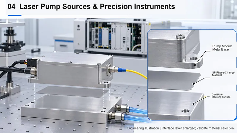
Figure 8. Engineering illustration for precision-instrument applications. The interface layer is enlarged for visibility; actual selection requires validation.
Sheen's application-sharing material lists laser-emitter pump sources as an application direction. In these systems, evaluate a thin phase-change interface between the heat-source mounting surface and cooling base. Where temperature stability matters, record the temperature distribution and mechanical assembly condition at the same time.
Near optical cavities, lenses, or other contamination-sensitive parts, request grade-specific silicone-free declarations, volatile or bleed data, and run material-compatibility evaluations. A series-level application introduction cannot prove cleanliness for each individual grade, and the words ‘precision instrument’ alone do not establish compatibility.
Choose the Material Route by Interface Job
| Interface Job | Route to Evaluate | Conditions to Confirm |
|---|---|---|
| Relatively flat, thin contact where interface resistance is the priority | SP phase-change material | Actual temperature, pressure, final BLT, and thermal history |
| Clear gaps or height differences across multiple devices | Gap-filling thermal pad or gel | Gap tolerance, compression range, and device load |
| High-voltage electrical isolation | Electrically insulating thermal material with suitable ratings | Withstand voltage, creepage distance, and system insulation design |
| Structural bonding and mechanical fixing | Confirmed thermally conductive adhesive solution | Bond strength, curing conditions, and rework requirements |
| Optical or silicone-sensitive environment | Solution with grade-level cleanliness evidence | Composition declaration, volatility, bleed, and compatibility |
Table 2. Select the material family by the job the interface must perform, then verify the specific grade in the actual assembly.
The inherent tack of SP material at room temperature helps with positioning; it does not make the sheet a structural adhesive. The three TDS documents also do not provide a complete electrical dataset for high-voltage isolation design. Low resistance creates value only when the material is assigned to the right interface task.
From Sample to Stable Production: Four Gates
Gate 1 — Define the Real Interface
Give Sheen the device model, contact area, upper and lower surface materials, flatness, installation gap, expected interface temperature, and allowable load. The TDS's 50 psi is a stated test condition, not a recommended assembly pressure for every device. Total heatsink fastening force also does not mean every region sees uniform pressure.
Gate 2 — Freeze the Assembly Method
Confirm the die-cut shape, thickness specification, and release-liner arrangement. Clean the contact surfaces using an approved process, then control placement, wrinkles, and foreign particles. Use a consistent fastening sequence and clamp condition. The TDS lists no preheating requirement for assembly, but that does not mean a low-temperature assembly has already reached stable post-phase-change thermal performance.
Gate 3 — Build a Repeatable Thermal Test
Verify test temperature, hold time after phase change, final BLT, and whether the nominal value includes contact effects on both sides. Compare the incumbent material and the three SP samples under identical power, ambient, and cooling conditions. Keep repeat samples and record scatter; one lucky low-temperature run is not a replacement decision.
Gate 4 — Validate Operation and Service
Use thermal cycling, power cycling, or high-temperature holds that reflect the equipment's real duty. Check temperature drift, material migration, interface coverage, and disassembly condition, then validate cleaning and replacement. Pump-out resistance, long-term maintenance-free operation, and target service life all need grade-, structure-, and test-specific evidence.
The TDS lists an operating range of −25 to 125 °C and a shelf life of 12 months for all three materials. If equipment, transport, or storage conditions move outside the confirmed range, request additional evaluation instead of borrowing another material's ratings. Production documents should also freeze the revision, batch traceability, incoming dimensions, and packaging method.
Start with Your Interface Conditions
A material fits a project only when it can transfer heat reliably in the real interface. Sheen's SP Series combines room-temperature sheet handling, heat-activated softening and wetting, and custom die-cutting, allowing R&D teams to evaluate thermal performance and assembly together from the first prototype.
If you are assessing a thin interface between a processor and heatsink, a network chip and thermal module, or a precision heat source and cooling base, contact Sheen for samples and technical documents for SP205A-60, SP205A-65-W4, and SP205A-80-W4. Include the incumbent material, device power, contact dimensions, actual pressure, temperature range, and the problem you want to solve so the comparison can be designed around your structure.
Sheen Thermal
Dongguan Sheen Electronic Technology Co., Ltd · Founded in 2008
Manufacturer of thermal interface materials and silicone foam for automotive electronics, energy storage, power electronics, communications and consumer electronics.
Certified
- ISO 9001:2015
- ISO 14001:2015
- IATF 16949:2016
What we supply
- Thermal conductivity Up to 90 W/m·K
- Thickness 0.3–10.0 mm
- Custom & samples Die-cut to drawing, 3–7 days
LAST:Nothing