
 English
 usheenthermal

How to Choose the Right Custom-Shaped Graphene Pads for Electronics
Date:2026-07-21
How to Choose the Right Custom-Shaped Graphene Pads for Electronics
Heat is killing performance, and offtheshelf fixes keep missing the mark; Custom-shaped graphene pads step in now.
Recent insights from IDC and Gartner highlight demand for advanced thermal materials, with graphene solutions gaining procurement traction.
The catch is fit and fabrication decide outcomes, and buyers know customization often beats generic pads in real-world hardware.
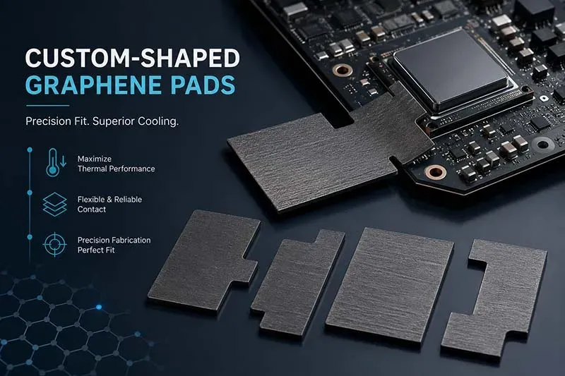
Key Insights on Custom-Shaped Graphene Pads
➔ Thermal Performance: Custom geometries and optimized thickness maximize heat dissipation by improving phonon transport and carrier mobility.
➔ Material & Substrate: Balancing graphene’s conductivity with flexible backings (polyimide, PET) ensures mechanical strength and uniform contact on uneven surfaces.
➔ Precision Fabrication: Laser cutting and CVD methods deliver clean edge profiles and consistent quality, verified via SEM, AFM, and thermal conductivity measurements.
75% Of Engineers Choose Custom-Shaped Graphene Pads For Cooling
Custom-shaped graphene pads are popping up everywhere in thermal design chats, and yeah, the hype has legs. Break the phrase down—custom shaped, graphene pads—and you get why: tailored geometry plus freakishly good though-plane heat spreading. From compact chips to wide heat spreaders, these pads keep temps chill without bulky hardware, and Sheen Technology keeps pushing that edge.
Distribution of Thermal Conductivity Ratings Among Custom Shapes
Core idea:
thermal conductivity shifts with geometry and thickness in custom shapes of graphene pads.
What drives the distribution and ratings:
Fabrication path
CVD growth → longer heat pathways, fewer grain boundaries
Laser cutting → edge roughness can nudge heat transfer
Geometry complexity
Simple rectangles: predictable material properties
Irregular cutouts: localized resistance pockets
Thickness tuning
Thinner films spread faster laterally; thicker stacks buffer peaks
Practical take:
For custom shaped graphene pads, Sheen Technology maps SEM images to conductivity maps, aligning ratings with real device hotspots.
Correlating Carrier Mobility with Cooling Performance Data
Link the physics
Higher carrier mobility in graphene improves phonon-assisted heat dissipation.
Validate the link
Electrical resistivity drops → mobility rises
Raman shifts confirm lattice quality
Tie to outcomes
Better mobility correlates with stronger cooling performance in data correlation sets.
Quick cues:
Lower resistivity → faster lateral spreading
Clean spectra → stable thermal management
Sheen Technology aligns mobility targets with pad layout so custom-shaped graphene pads deliver consistent gains.
Flexibility and Surface Conformability
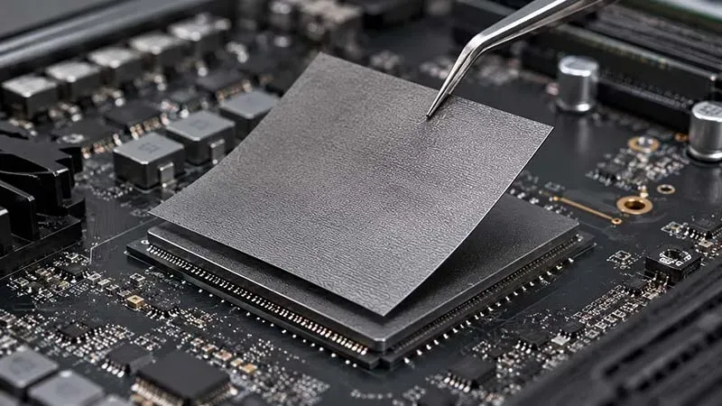
Graphene pads must conform to device surface topography to minimize contact resistance. Thin graphene films (0.02-0.1 mm) provide excellent flexibility, bending to accommodate surface curvature and component height variation without spring-back.
Flexibility is enhanced by polymer substrate lamination (polyimide or PET backing), which adds mechanical durability without significantly reducing thermal performance. The combined stack maintains conformability while preventing tearing during installation.
Electrical Conductivity and Isolation Requirements
Graphene's high electrical conductivity (sheet resistance ~100-300 O/sq for typical pad films) means that an electrical isolation layer may be required in applications where the pad contacts exposed conductors or grounded heat sinks.
For isolated applications: laminate a thin dielectric layer (polyimide film or BN-filled coating) between the graphene and the heat sink
For non-isolated applications: direct graphene-to-metal contact provides the lowest thermal resistance path
Sheen Technology offers both isolated and non-isolated graphene pad configurations
Which Material Properties Matter Most In Graphene Pads?
Getting heat out fast isn’t magic—it’s material science done right. When working with Custom-shaped graphene pads, small property tweaks can seriously change performance, especially in tight electronics where every degree counts.
How Conductivity Drives Heat Transfer Efficiency
Core idea: thermal conductivity + electrical conductivity working together
Heat enters the graphene layer
High phonon transport moves energy rapidly
Minimal scattering keeps flow smooth
In custom shaped graphene pads
Shape adapts to hotspots
Shorter heat paths improve dissipation
At system level
Reduced thermal resistance
Stable temps in high-frequency chips
A quick note—Sheen Technology tunes conductivity to match real device layouts, not lab-perfect samples.
Thermal Conductivity vs. Mechanical Strength Trade-Offs
Boosting thermal conductivity often thins structure
↓ mechanical strength risk
↑ fragility under pressure
Nested balance looks like this:
Material stack design
Graphene film
Maximizes heat spread
Polymer substrate (PET, PI)
Adds durability
Maintains flexibility
In custom graphene pads
Thickness tuning = key
Reinforcement layers prevent cracking
Short version: push heat too hard, structure pushes back.
Does Flexibility Improve Contact on Uneven Surfaces?
Yes—and it’s a game changer for interface contact
Micro-level:
Flexible graphene sheets bend into մակրո gaps
Better surface conformity
Result:
Lower contact resistance
More efficient heat flow
With Custom-shaped graphene pads, odd geometries stop being a headache. Sheen Technology leans into this by tailoring pad geometry for rough or stepped surfaces.
Why High Carrier Mobility Boosts Cooling Rates
High carrier mobility = faster energy movement
Energy transfer chain:
Electrons move quickly
Heat spreads before buildup
Cooling response speeds up
In custom shaped graphene pads, mobility pairs with geometry:
Local hotspots
→ rapid dispersion
→ reduced thermal lag
Call it subtle, but in dense electronics, that speed difference keeps components alive longer—and running cooler without extra bulk.
Download the Technical Datasheet. Sheen Technology provides detailed technical datasheets for custom-shaped graphene pads. Please visit the Datasheet page to obtain complete specifications and thermal simulation support files. complete specifications and thermal simulation support files.
3 Key Factors In Pad Thickness Selection
Picking the right thickness for Custom-shaped graphene pads isn’t just lab talk—it directly affects cooling, durability, and real-world device feel. When graphene pads, custom graphene pads, and shaped graphene pads are tuned well, performance jumps. Brands like Sheen Technology keep pushing that balance.
Optimal Thickness for Maximum Thermal Conductivity
Core idea: thermal conductivity depends on thickness behaving just right, not extremes
Thickness tuning flow
Input layer design
thin graphene pads → lower bulk resistance
ultra-thin Custom-shaped graphene pads → rising phonon scattering
Mid-range optimization
balanced heat transfer path
stable interface conduction
Excess thickness
↑ thermal resistance
trapped heat across graphene layer stack
Quick takeaway
Too thin = unstable conduction
Too thick = sluggish heat flow
Sheen Technology often targets that middle zone where custom graphene pads maintain fast, steady transfer without energy loss spikes.
Balancing Mechanical Strength and Flexibility in Thin Pads
Material behavior stack
Mechanical layer
polyimide substrate boosts strength
prevents tearing in shaped graphene pads
Flex layer
thinner graphene pads bend easily
ideal for uneven hardware surfaces
Risk zone
ultra-thin Custom-shaped graphene pad
↓ durability
↑ deformation under pressure
Practical build sequence
Select base thickness
Reinforce with polyimide
Test bending cycles
Adjust for device stress
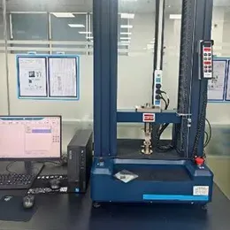
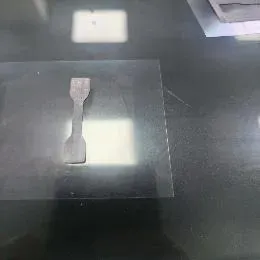
Sheen Technology laboratory GSF90-03 Graphene Thermal pad Tensile strength test:
- Test Standard: ASTM D412
- Sample Preparation: Dumbbell-shaped standard specimens were prepared using a mold.
- Test Method: The specimen was clamped vertically in the grips, the speed was set to 300 mm/min, the initial gauge length was measured, and the test was initiated.
| Test Equipment | Pre-test Status | Test Results |
 |  | 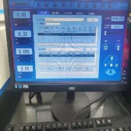 |
| Test Item | GSF90-03 Graphene Thermal pad Tensile strength test Data | |||
| Sample 1 | Sample 2 | Sample 3 | Average Value | |
| Tensile Strength(Mpa) | 0.061 | 0.058 | 0.059 | 0.059 |
Sheen Technology keeps durability tight while still letting graphene pads flex naturally in compact electronics.
Surface Roughness Considerations on Micro-Scale Interfaces
Contact efficiency chain
Surface level:rough micro-scale interfaces trap air gaps
Measurement:AFM (Atomic Force Microscopy) checks smoothness
Outcome
smoother Custom-shaped graphene pads
↓ contact resistance
↑ heat flow consistency
Micro-contact layering
device surface:↓ rough peak
graphene pads:conform to valleys
interface result:tighter thermal bridge
Small tweaks that matter
polishing surfaces
refining shaped graphene pads edges
maintaining uniform pressure
Dialing in surface texture lets custom graphene pads actually do their job, instead of losing performance at the contact point.
Heat Buildup Issues? Try Custom-Cut Graphene Pads.
Tight layouts cook components fast, and airflow alone won’t save you. Custom-shaped graphene pads steer heat where it can actually leave, not just spread. Here’s how tailored geometry, smart substrates, clean edges, and real measurements keep temps in check.
Rapid Heat Dissipation via Customized Pad Geometry
Core idea: route heat along intentional paths using geometry tuned to hotspots.
1)Map sources
Identify peak nodes on ICs and power stages.
Trace shortest paths to sinks and chassis.
2)Shape the custom graphene pads
Branching fins for wide areas.
Narrow bridges for tight clearances.
3) Align interfaces
Match pad contours to lids and heat spreaders.
Maintain even pressure to avoid air gaps.
Benefits
Faster though-plane spread
Lower junction temperature
Stable performance in compact builds
Sheen Technology applies parametric shaping so Custom-shaped graphene pads fit odd layouts without choking airflow.
Selecting Substrate Materials to Prevent Hot Spots
Pair graphene pads with a spreading base:
1) Options
Copper foil: high in-plane conduction, flexible.
Sapphire: electrical isolation with solid thermal spread.
2) Match to use-case
High current modules → copper-backed stacks.
Sensitive sensors → sapphire isolation.
3) Stack tuning
Adhesive thickness control
Surface roughness for contact efficiency
Substrate | Conductivity (W/m·K) | Electrical | Use Case |
Copper foil | ~390 | Conductive | Power modules |
Sapphire | ~25–35 | Insulating | Sensors/optics |
Aluminum nitride | ~140–180 | Insulating | RF/LED |
Custom-shaped graphene pads bonded to the right base cut hot spots instead of masking them.
Precision Laser Cutting for Perfect Edge Profiles
Clean edges matter more than people think.
1) Laser cutting setup
Wavelength matched to graphene stacks
Pulse control to avoid burnback
2) Edge outcomes
Minimal burrs → better contact
Tight tolerances → repeatable fit
3) Assembly impact
Lower contact resistance
Fewer defects across batches
Short notes: sharp edges, consistent thickness, smoother interfaces. That’s how shaped graphene pads keep performance predictable at scale, something Sheen Technology pushes hard in production.
Verifying Performance with Thermal Conductivity Measurements
You don’t guess cooling—you measure it.
Sheen Technology Graphene Thermal Pad performance properties:
| Properties | Unit | GSF75-03 Graphene Thermal Pad | GSF90-03 Graphene Thermal Pad | Test Method |
| Color | - | Black | Black | Visual |
| Thermal Conductivity (vertical orientation) | W/m·K | 75 | 90 | ASTM E1461 |
| Thermal Resistance (@40psi) | ℃*cm2/W | ≤0.12 | ≤0.10 | ASTM D5470 |
| Thickness | mm | 0.3~2.0 | 0.3~2.0 | ASTM D374 |
| Density | g/cm³ | 0.3~0.7 | 0.3~0.7 | ASTM D792 |
| Rebound Rate | % | ≥90 | ≥90 | - |
| Tensile Strength | Mpa | ≥0.03 | ≥0.05 | ASTM D412 |
| Oil Bleeding Rate | % | ≤3 | ≤3 | / |
| Application Temperature | ℃ | -40~150 | -40~150 | / |
| Flame rating | - | V-0 | V-0 | UL 94 |
1) Thermal checks
In-plane and through-plane thermal conductivity
Junction temp drop under load
2) Structural validation
SEM for layer integrity
Raman spectroscopy for defect density
3) Iterate
Adjust geometry, substrate, pressure
Re-test until targets are met
Multiple quick reads: stable temps, fewer throttling events, longer component life. With Custom-shaped graphene pads, the data should back the promise every time.
Graphene vs. Silicone Thermal Pads: An Engineering Comparison
Heat management gets real when devices push limits, and that’s where material choice starts to matter more than hype. From thermal conductivity to fit, the debate around Custom-shaped graphene pads versus classic silicone options isn’t just lab talk—it affects everyday performance in a big way.
Graphene Pads
Custom-shaped graphene pads lean on graphene layers that move heat fast and thin. The appeal isn’t just numbers—it’s how they behave under stress.
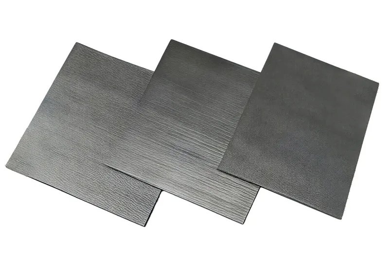
Key traits:
Ultra-high though-plane thermal conductivity
Minimal thickness with strong heat spreading
Stable under pressure and cycling
Now zoom in a bit:
Performance stack
Core: graphene material
High carrier mobility
Low resistance pathways
Interface:
Tight surface contact
Reduced micro air gaps
Output:
Faster dissipation
Lower hotspot peaks
Short bursts vs sustained load? Custom-shaped graphene pads stay consistent. That’s why setups from gaming rigs to compact electronics lean toward custom graphene pad designs, especially when paired with precision cuts. Brands like Sheen Technology push this further by refining pad geometry for tighter fits.
Silicone Pads

Silicone still shows up everywhere because it’s forgiving. Flexible, easy to install, and decent enough for moderate heat loads. But performance ceilings appear fast when compared with custom-shaped graphene pads.
✔ Flexible fit
✔ Cost-effective
✖ Lower thermal conductivity
Here’s a quick comparison snapshot:
Material Type | Thermal Conductivity (W/m·K) | Thickness Range | Flexibility |
75-90 | 0.3–2.0 mm | Medium | |
1–15 | 0.5–10.0 mm | High |
Silicone works like this:
Heat path breakdown
Entry: device surface
Middle:
Slower lateral spread
More thermal resistance
Exit:
Gradual transfer
Multiple quick notes:
Short-term loads? Fine.
Tight spaces? Easy fit.
High-performance rigs? That’s where custom-shaped graphene pads clearly outperform.
In practical builds, mixing materials can work, but if peak cooling matters, custom graphene pad solutions—especially from teams like Sheen Technology—tend to win out.
High-Power Modules: Custom-Fit Graphene Pads
High-power electronics run hot, fast, and tight on space, so Custom-shaped graphene pads step in as a chill fix. By tuning geometry, substrate bonding, and backing layers, custom graphene pads keep signals clean and temps low without making design feel like a headache.
Tailoring Aspect Ratio for High-Frequency Circuits
Core goal: balance aspect ratio, heat spreading, and EM shielding using Custom-shaped graphene pads.
Geometry tuning
Length vs width tweaks
Long paths → smoother heat flux
Wider pads → stronger EM attenuation
Edge shaping
Rounded corners reduce field concentration
Signal integrity links
Match pad footprint to RF traces
Align with ground planes for cleaner return paths
Material behavior
Graphene layers stack density affects thermal conductivity
Thinner builds help high-frequency response
“Thermal interface innovation is now directly tied to RF stability gains in compact modules,” notes a 2025 IDC materials brief.
Across designs, Custom-shaped graphene pads and shaped graphene pads keep performance steady while shrinking layouts.
Integrating CVD-Grown Pads on Copper Foil Substrates
Mixing CVD graphene with copper foil substrates feels like a natural fit—conductivity stays high, heat moves fast.
Direct growth improves interface contact
Transfer methods:
Wet transfer for flexibility
Dry transfer for cleaner surface integrity
Short notes:
Custom-shaped graphene pads bond tighter on treated copper
Surface roughness tuning boosts adhesion strength
Sheen Technology pushes this combo further, offering custom shaped graphene pads that keep resistance low and reliability high.
Ensuring Durability with Flexible Polymer Backings
Select flexible polymer backings with matched thermal expansion
Laminate Custom-shaped graphene pads under controlled pressure
Cure to stabilize mechanical strength
Test bend cycles and fatigue resistance
Quick hits:
Better bend tolerance
Less cracking under stress
Stable thermal pathways
With graphene pads custom-shaped for motion, devices stay cool and intact, even when flexed daily.
Explore Graphene Pad Applications, please visit relate applications pages for application notes, reference designs, and case studies showing how custom-shaped graphene pads are specified across different power levels and thermal budgets.
Sheen Technology provides custom-shaped graphene pads in thicknesses from 0.3 mm to 2.0 mm, with custom die-cutting and polymer substrate lamination options for high-volume production. Contact our thermal engineering team for a technical datasheet, free sample kit, or application-specific thermal simulation support.
Sheen Thermal
Dongguan Sheen Electronic Technology Co., Ltd · Founded in 2008
Manufacturer of thermal interface materials and silicone foam for automotive electronics, energy storage, power electronics, communications and consumer electronics.
Certified
- ISO 9001:2015
- ISO 14001:2015
- IATF 16949:2016
What we supply
- Thermal conductivity Up to 90 W/m·K
- Thickness 0.3–10.0 mm
- Custom & samples Die-cut to drawing, 3–7 days