
 English
 usheenthermal

How to Use the GPU Thermal Pad Thickness Chart: 1.0 / 1.5 / 2.0 / 3.0mm
Date:2026-09-23
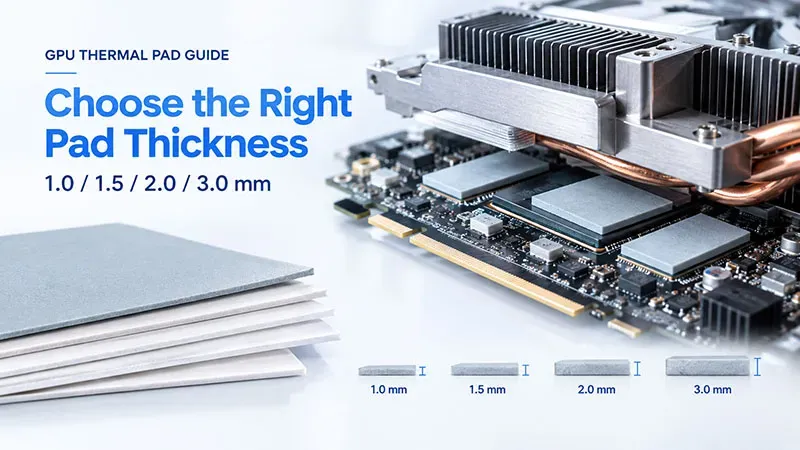
GPU Thermal Pad Thickness Chart: 1.0 / 1.5 / 2.0 / 3.0mm tackles a tiny measurement with big consequences: poor contact, excess pressure, or lousy cooling. Thickness alone won’t save the day.
Sheen Technology’s official guidance treats thickness, hardness, compression, and thermal performance as linked specification factors.
This guide turns measured GPU gaps into practical pad choices, then connects engineering validation with repeatable production purchasing decisions.
Key Points for GPU Thermal Pad Thickness Chart: 1.0 / 1.5 / 2.0 / 3.0 mm
- Match pad thickness to measured GPU gap—1.0 mm for tight VRAM clearances, 1.5 mm for MOSFETs, 2.0 mm for chipsets, 3.0 mm for multi-chip spans.
- Consult material specs: thermal conductivity, dielectric breakdown, Shore hardness, and compression tolerance for reliable contact and insulation.
- Use calibrated gauges and clean heatsink surfaces to confirm uniform gap, then verify contact with a reference sheet before pad installation.
- Source via bulk procurement: require technical datasheets, RoHS/REACH compliance, UL94 V-0 rating, thickness tolerance, and lot traceability for consistent performance.
GPU Thermal Pad Thickness Chart Explained
A GPU Thermal Pad Thickness Chart helps match pad size to the actual component-to-heatsink gap. Getting that fit right supports GPU cooling without overdoing mounting force, while material specs help buyers avoid headaches when sourcing replacement or production pads.
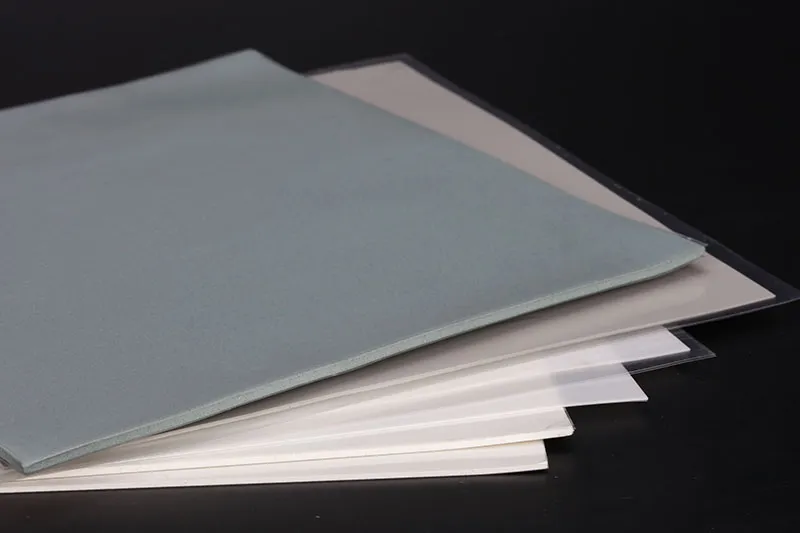
Thermal Conductivity and 1.0–3.0mm Thickness Overview
GPU Thermal Pad Thickness choices should start with a measured gap, not a best guess.
Gap fit
- A 1.0mm pad suits small clearances where firm contact is possible.
- A 1.5mm pad adds reach while keeping mounting pressure manageable.
- A 2.0mm pad handles wider component gaps.
- A 3.0mm pad works for deep clearances but needs suitable compression.
Thermal performance
- Higher thermal conductivity can improve heat dissipation.
- Correct thermal pad thickness matters just as much; excess thickness can raise thermal impedance by creating too much mounting force.
In short, measure twice and fit once.
Key Material Properties: Dielectric Breakdown & Shore Hardness
A GPU thermal pad also needs safe electrical and mechanical behavior.
- Check dielectric breakdown ratings for adequate electrical insulation around VRAM and MOSFETs.
- Compare shore hardness with compressibility.
- Softer silicone material can settle around uneven parts.
- Greater material flexibility improves surface contact, though overly soft material may deform during assembly.
These properties help keep contact snug without putting unnecessary stress on the board.
Supply Chain Essentials: Technical Datasheet & Bulk Procurement
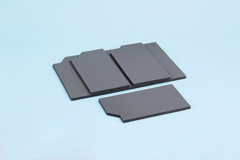
Before buying GPU thermal pads in volume, verify the paperwork and production controls. Sheen Technology provides selection data sheets for thermal pads of various thicknesses:
| Properties | Color | Thermal Conductivity | Thermal Impedance (1mm,@30psi) | Thickness | Standard Hardness | Customized Hardness |
| Unit | - | W/m·K | ℃*in²/W | mm | Shore 00 | Shore 00 |
| SF100 | Gray White | 1.5 | 0.90 | 0.3 ~ 10.0 | 40/60±5 | 10 ~ 90 |
| SF300 | Dark Gray | 2.0 | 0.70 | 0.3 ~ 10.0 | 40/60±5 | 10 ~ 90 |
| SF400 | Yellow | 2.5 | 0.50 | 0.3 ~ 10.0 | 40/60±5 | 10 ~ 90 |
| SF500 | Blue | 3.0 | 0.45 | 0.3 ~ 10.0 | 40/60±5 | 20 ~ 90 |
| SF600D | Gray | 4.0 | 0.40 | 0.3 ~ 5.0 | 40/60±5 | 30 ~ 90 |
| SF600 | Gray/Pink | 5.0 | 0.35 | 0.5 ~ 5.0 | 40/60±5 | 30 ~ 90 |
| SF600G | Gray | 6.0 | 0.30 | 0.5 ~ 5.0 | 40/60±5 | 30 ~ 90 |
| SF700 | Gray | 7.0 | 0.25 | 0.5 ~ 5.0 | 40/60±5 | 30 ~ 90 |
| SF800 | Gray | 8.0 | 0.22 | 0.5 ~ 5.0 | 40/60±5 | 30 ~ 90 |
| SF1000 | Gray | 10.0 | 0.18 | 0.5 ~ 5.0 | 40/60±5 | 30 ~ 80 |
| SF1200 | Gray | 12.0 | 0.15 | 0.8 ~ 5.0 | 40/60±5 | 30 ~ 80 |
| SF1500 | Gray | 15.0 | 0.10 | 1.0 ~ 5.0 | 40±10 | 30 ~ 60 |
Documentation
- Review the technical datasheet for conductivity and thickness tolerance.
- Confirm the material specification covers UL94 V-0, RoHS, REACH, and halogen-free requirements where applicable.
Production
- Check quality control procedures and relevant manufacturing standards.
- Match sheets, rolls, or die-cut parts to real procurement parameters.
Long-term supply
- Monitor batch consistency across the supply chain.
- Stable dimensions and material performance support predictable product reliability.
4 Steps To Measure GPU Gap Precisely
Getting GPU spacing right prevents weak contact and excess pad pressure. A GPU Thermal Pad Thickness Chart gives useful starting sizes, but actual gaps still need checking. Sheen Technology recommends measuring each contact area separately. Small differences matter, so accurate tools, clean surfaces, controlled reference materials, and clear records keep the job on track.
Selecting the Right Gauge for Accurate Measurements
A GPU Thermal Pad Thickness Chart should guide selection, not replace measurement.
Gauge choice
- Use a calibrated digital caliper or micrometer where access permits.
- For narrow spaces, a thickness gauge can be the better measuring tool.
This keeps 1.0mm, 1.5mm, 2.0mm, and 3.0mm choices grounded in measured clearance rather than guesswork.
Preparing the GPU Heatsink Surface for Consistent Contact
Clean contact areas before measuring.
Remove old thermal paste and loose surface residue.
- Apply isopropyl alcohol with a lint-free microfiber cloth.
- Avoid leaving excess cleaning agent behind.
Inspect the copper baseplate.
- Check flatness at several points.
- Recheck any spot that looks warped or nicked.
A clean base gives the GPU Thermal Pad Thickness Chart a reliable physical reference.
Using a Graphene Thermal Sheet as a Reference Gap Filler
A known graphene sheet works as a thin reference material when verifying contact.
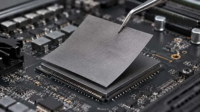
Contact check
- Place the test sample without forcing the assembly.
- Inspect contact distribution after closing.
- Note visible deformation.
- Compare it with the intended compression rate.
Graphite offers high thermal conductivity, but it behaves differently from a soft silicone gap filler. That distinction matters when converting observed clearance into a thermal pad thickness.
Documenting Results for Quality Inspection and ISO Standard Compliance
Good records make repeat builds much easier, especially when Sheen Technology production checks need traceability.
Measurement data
- Log each GPU location and measured gap.
- Match it against the GPU Thermal Pad Thickness Chart: 1.0 / 1.5 / 2.0 / 3.0mm.
Quality control
- Record compression targets in the specification sheet.
- Add batch and pass/fail results to the inspection report.
Traceability
- Maintain an audit trail through controlled documentation.
- Link tolerances and inspection methods to applicable standard compliance procedures.
4 Scenarios: 1.0–3.0mm Pad Applications
Matching pad thickness to the measured hardware gap keeps cooling practical and mounting pressure sane. This GPU Thermal Pad Thickness Chart guide covers four common fits.
VRAM Module Cooling with a 1.0mm Thermal Pad
For a VRAM module, a 1.0mm thermal pad suits a tight measured gap between video memory and the cooler.
Check the fit:
- Confirm full surface contact after assembly.
- Keep compression moderate; squashing the gap filler too hard may affect GPU cooling.
Check performance:
- Higher thermal conductivity supports better heat dissipation.
- Electrical insulation matters around exposed components.
Sheen Technology recommends selecting thickness from actual clearance rather than the card model alone. Keep the GPU Thermal Pad Thickness Chart handy.
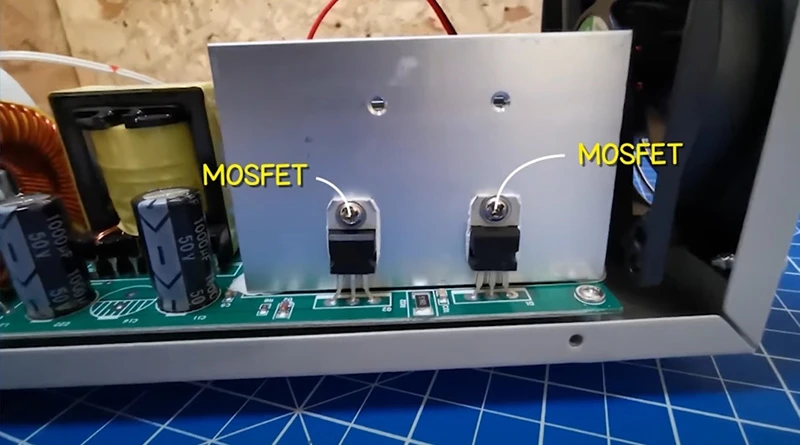
Power MOSFET Heat Dissipation Using 1.5mm Material
A power MOSFET often benefits from 1.5 mm material when voltage regulator heights vary slightly. For VRM cooling, the pad should conform without forcing the heat sink upward.
| Pad | Example gap | Compression | Typical role |
| 1.0mm | 0.8–0.9mm | 10–20% | VRAM |
| 1.5mm | 1.2–1.35mm | 10–20% | MOSFET |
| 2.0mm | 1.6–1.8mm | 10–20% | Chipset |
| 3.0mm | 2.4–2.7mm | 10–20% | Large gap |
These are fit examples, not universal specifications. Pad hardness changes compression, so verify the thermal interface and temperature control after mounting.
Graphics Card Chipset Cooler Interface at 2.0mm Thickness
A graphics card with a larger chipset gap may call for 2.0 mm thickness.
Measure the cooler interface clearance.
- Account for normal thermal pad compression.
- Avoid excess mounting pressure.
Reassemble carefully.
- Confirm the GPU core still contacts its cooler correctly.
That makes the GPU Thermal Pad Thickness Chart a starting point, while measurements settle the final choice.
High-Performance Multi-chip Builds with 3.0mm Gap Fillers
A multi-chip build can have a large clearance that thinner pads simply cannot bridge. A 3.0mm gap filler provides extra reach and compliance.
- For fit: A soft compressible pad can handle component-height differences during hardware assembly.
- For cooling: Greater thickness can increase thermal resistance, so thermal management still depends on conductivity, compression, and contact quality.
For a high-performance build, Sheen Technology pad selection should balance gap coverage with low thermal resistance rather than assuming thicker is automatically better.
Data Shows 2.0mm Pads Cut Temps By 10%
The GPU Thermal Pad Thickness Chart gives buyers a practical starting point, but real cooling gains still come down to fit, pressure, materials, and operating conditions.
Thermal Conductivity Impact on Temperature Reduction
A higher thermal conductivity can improve heat transfer, but conductivity alone cannot promise a 10% temperature reduction.
Real cooling performance also depends on:
- thermal resistance across the pad and interfaces.
- Contact area, airflow, heat load, and pad compression.
Lower junction temperature signals better heat dissipation, yet results remain test-specific.
For GPU Thermal Pad Thickness Chart, Sheen Technology recommends checking the actual gap rather than simply chasing the highest conductivity rating. It’s a small detail, but it matters.
Benchmarking 2.0mm Pads vs. 1.5mm and 3.0mm Thicknesses
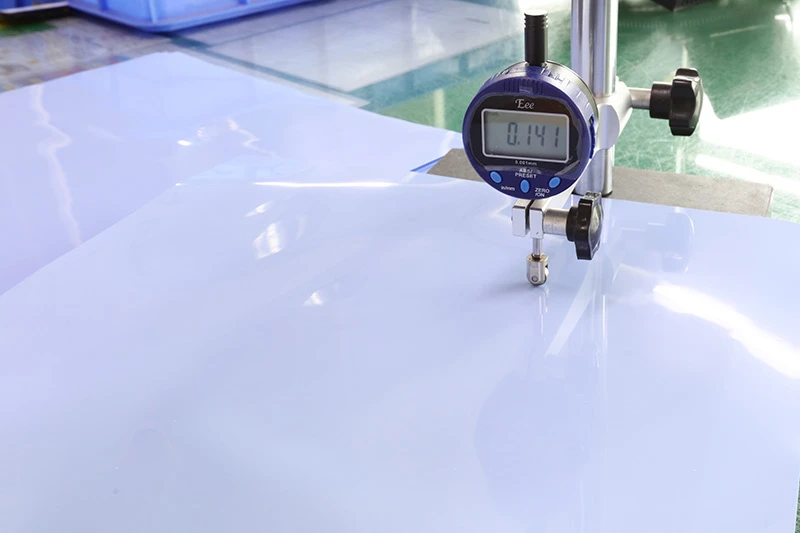
For fair benchmark testing, keep GPU load, room temperature, material conductivity, and mounting pressure unchanged.
- Measure the gap before selecting pad thickness.
- Compare 1.5mm, 2.0mm, and 3.0mm using equal test conditions.
- Check the compression rate and contact marks after mounting.
A 2.0mm pad can deliver stronger thermal performance when gap filling is correct. Too thin may lose contact; too thick may create excess pressure. That’s the key takeaway behind a GPU Thermal Pad Thickness Chart for practical GPU cooling and hardware testing.
Bulk Procurement Advantages for Halogen-Free, RoHS-Compliant Pads
Bulk purchasing can simplify sourcing and improve lot consistency.
Buyers should specify:
- halogen-free requirements and RoHS compliance.
- Approved material composition and manufacturing standards.
- Release liners, packaging, inspections, and lot traceability.
For Sheen Technology orders, pairing a GPU thermal pad thickness guide with documented environmental safety requirements helps procurement teams source eco-friendly materials without losing sight of thermal fit or quality control.
【Request a Custom Quote】Choosing between 1.0mm, 1.5mm, 2.0mm, and 3.0mm pads for VRAM, MOSFETs, chipsets, or multi-chip builds? Send us your gap measurements by location, available clamp pressure, the isolation voltage the joint must withstand, and your target thermal impedance, and our engineers can recommend the thickness and hardness grade your GPU thermal pad thickness chart calls for.
Sheen Thermal
Dongguan Sheen Electronic Technology Co., Ltd · Founded in 2008
Manufacturer of thermal interface materials and silicone foam for automotive electronics, energy storage, power electronics, communications and consumer electronics.
Certified
- ISO 9001:2015
- ISO 14001:2015
- IATF 16949:2016
What we supply
- Thermal conductivity Up to 90 W/m·K
- Thickness 0.3–10.0 mm
- Custom & samples Die-cut to drawing, 3–7 days