
 English
 usheenthermal

Overcoming Power Density in Semiconductor Test Equipment Thermal Design
Date:2026-09-17
Semiconductor test equipment thermal design now faces a hot little headache: more watts, tighter spaces, and nasty hot spots. Cooling alone won’t save the day.
SEMI forecasts 2025 semiconductor manufacturing equipment sales at $125.5 billion, raising the stakes for repeatable thermal performance and scalable material sourcing.
That puts interface materials, substrates, spreaders, insulation, and seals under the microscope—because every thermal path matters.
Quick Insights: Harmonizing Semiconductor Test Equipment Thermal Design
➔ Leverage ceramic substrates (aluminum nitride, SiC) for low-resistance, electrically isolated thermal paths.
➔ Deploy phase-change materials at chip interfaces to absorb spikes and stabilize junction temperatures.
➔ Integrate heat-flux sensors or IR arrays to pinpoint hot spots and validate cooling layouts.
➔ Opt for copper-tungsten base plates plus graphite sheets to spread and lateralize heat efficiently.
➔ Choose modular liquid cold-plate networks or microchannel coolers for scalable, high-density heat rejection.
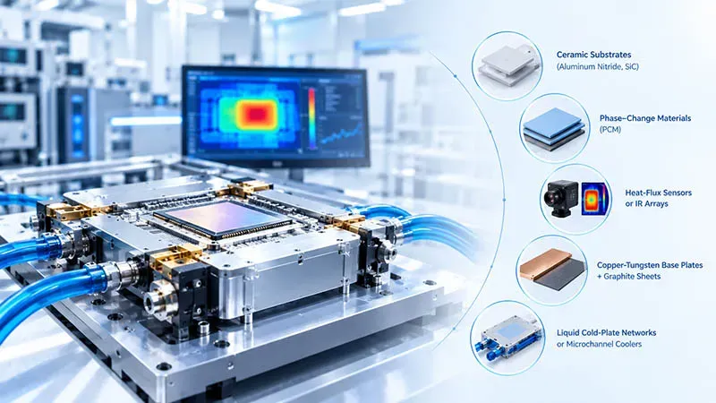
Note: This image was generated with the assistance of AI; it is not a real photograph and is for reference only.
Key Thermal Challenges In Semiconductor Test Equipment
High-power semiconductor test equipment thermal design has a tough job: move heat fast, keep electrical paths safe, and hold test temperatures steady. Good semiconductor thermal design connects materials, sensing, and insulation so test equipment can handle rising loads without throwing measurement accuracy off course.
Tackling Thermal Resistance with Ceramic Substrate Interfaces
A ceramic substrate can cut thermal resistance while preserving electrical isolation. For high power density, that’s a big deal. Interface choices should match:
Material performance
- Aluminum nitride offers strong thermal conductivity for rapid heat dissipation.
- Silicon carbide suits demanding semiconductor packaging conditions.
Assembly needs
- A thin interface material closes small air gaps that otherwise trap heat.
For semiconductor test equipment thermal design, Sheen Technology can pair boron nitride thermal pad with cooling hardware to create shorter, steadier heat paths.
Mitigating Thermal Spikes via Phase Change Materials
A phase change material acts like a temporary heat buffer. During a thermal spike, it uses latent heat for heat absorption, slowing the temperature jump.
- Place the material close to the main heat source.
- Match its transition range to expected test temperatures.
- Check recovery between repeated transient thermal loads.
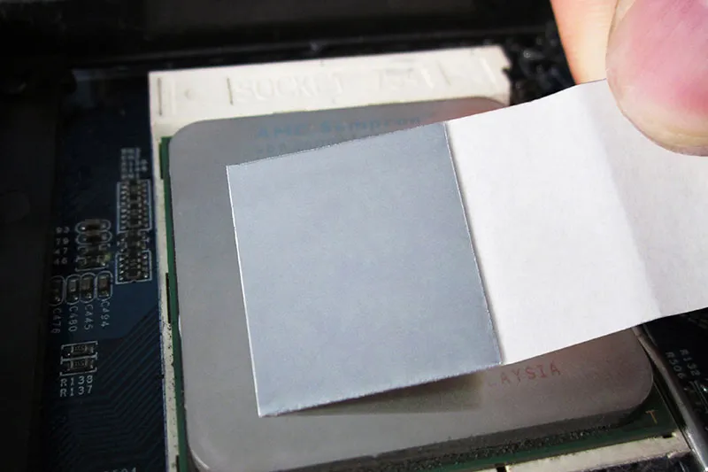
That simple approach supports temperature stabilization without making thermal management hardware needlessly bulky.
Managing Hot-Spot Formation Using Heat Flux Sensors
A small hot-spot can skew semiconductor test results long before the whole assembly looks overheated. A heat flux sensor supports real-time detection.
Engineers compare thermal gradient changes across the contact area.
- Thermal mapping shows where energy is moving.
- Temperature monitoring confirms the resulting surface response.
Finding localized heating early helps Sheen Technology tune cooling contact and airflow rather than chasing unstable readings later.
Preventing Insulation Breakdowns with Polyimide Film
Thin polyimide film adds electrical isolation where conductive parts sit close together, yet avoids the bulky heat barrier associated with heavy thermal insulation.
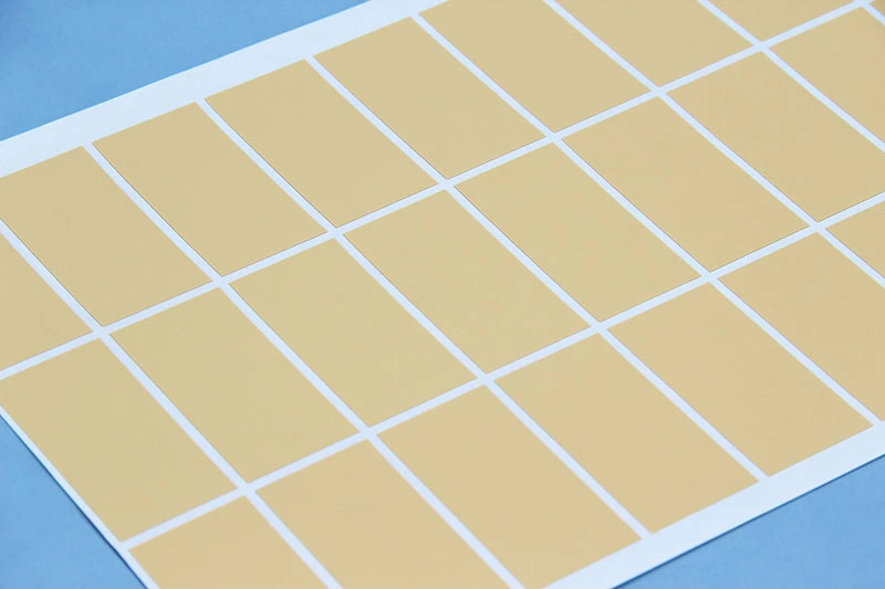
For safer semiconductor thermal design, three checks matter: verify dielectric strength, control film thickness, and inspect edges exposed to high-temperature cycling. These steps lower insulation breakdown risk while supporting long-term reliability.
4 Steps To Optimize Heat Sinks
Good semiconductor cooling starts with materials, interfaces, coolant paths, and surface protection working together. In semiconductor test equipment thermal design, these choices help control hot spots and device temperatures. Sheen Technology applies this practical thermal design approach to demanding test hardware.
Material Selection: Copper Tungsten Alloy Base Plates
Copper tungsten alloy makes a capable Base plate for high Power-density loads.
- High Thermal conductivity spreads concentrated heat.
- A controlled Coefficient of thermal expansion helps match device materials, while Mechanical stability supports repeatable contact in Semiconductor test equipment.
That balance matters when semiconductor test equipment thermal design must stay accurate through repeated heating cycles.
Surface Enhancement through Graphite Sheet Integration
A Graphite sheet adds Surface enhancement without much bulk. Its Anisotropic thermal conductivity moves heat sideways quickly. In contrast, graphene thermal sheets utilize a vertically oriented structure, allowing for rapid heat conduction along the thickness direction.
- Used as a Thermal interface material, Graphene Thermal sheets can lower Contact resistance.
- Better spreading supports Heat dissipation and steadier Thermal management, especially around concentrated test loads.
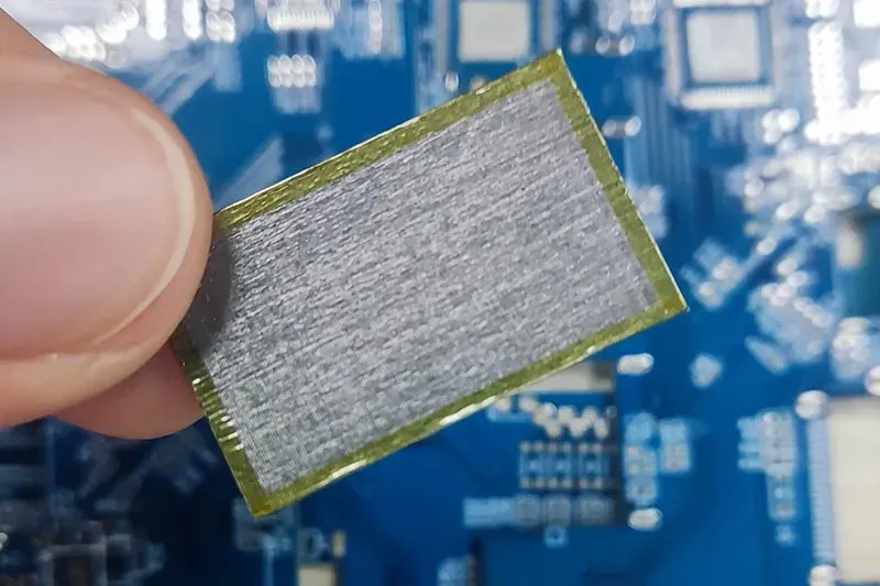
It’s a handy fix when ordinary thermal design leaves stubborn hot spots.
Channel Geometry: Designing Microchannel Cooler Fins
A Microchannel cooler puts coolant close to the heat source.
- Smaller Channel width can raise the Heat transfer coefficient.
- Practical Fin geometry must also respect Fluid dynamics.
- Excess restriction increases Pressure drop.
- Balanced flow improves Cooling efficiency without pushing pump demand too far.
Coating Application: Dielectric Coating for Corrosion Resistance
A Dielectric coating provides Electrical insulation while supporting Corrosion resistance.
Surface passivation limits coolant-driven attack, while Oxidation prevention protects exposed metal. In semiconductor test equipment thermal design, this added Environmental protection can preserve long-term Reliability without changing the core cooler geometry.
Air Vs. Liquid Cooling Solutions
Choosing cooling for semiconductor test equipment thermal design comes down to heat density, control, maintenance, and cost. Air handles modest test loads with little fuss, while liquid systems carry concentrated heat away when tighter semiconductor thermal design matters.
Air Cooling
Air cooling keeps semiconductor test equipment thermal design fairly simple.
Thermal path
- A heat sink spreads device heat through carefully selected fin geometry.
- An axial fan raises airflow velocity, improving convective heat transfer.
Operating limits
- Rising ambient temperature cuts cooling headroom.
- Higher thermal resistance can make dense semiconductor test equipment thermal design run hot.
Service is straightforward, which is handy for test equipment needing quick fan or sink replacement.
Liquid Cooling
Liquid cooling steps up when semiconductor test equipment thermal design faces concentrated loads. A cold plate collects heat through thermal interface material, while a coolant pump drives fluid through a fluid manifold and heat exchanger.
Typical engineering comparisons look like this:
| Cooling case | Heat load | Flow rate | Pressure drop | Computed coolant rise ΔT = Q/ṁ·cp (water) |
| Low load | 200 W | 0.5 L/min | 8 kPa | ≈ 5.7 K |
| Medium | 400 W | 1.0 L/min | 15 kPa | ≈ 5.7 K |
| High | 600 W | 1.5 L/min | 24 kPa | ≈ 5.7 K |
| Dense | 800 W | 2.0 L/min | 34 kPa | ≈ 5.7 K |
| Extreme | 1000 W | 2.5 L/min | 46 kPa | ≈ 5.7 K |
*These are engineering comparison values, not universal specifications.
Can We Predict Hot Spots Accurately?
Hot spots can shift in seconds as test power changes, so a single reading rarely tells the whole story. Good semiconductor test equipment thermal design combines surface maps, contact measurements, and calibrated models. Put simply, several data sources help engineers catch heat buildup before device results drift.
Leveraging Infrared Sensor Arrays for Real-Time Mapping
Infrared sensors support thermal imaging of each semiconductor die, turning emitted infrared energy into a visible temperature distribution.
Fast mapping
- Real-time monitoring tracks temperature during changing loads.
- Higher spatial resolution makes hot spot detection sharper.
Design feedback
- Semiconductor test equipment thermal design can compare maps across sockets and cooling interfaces.
- Semiconductor test thermal design teams can then adjust airflow or contact pressure. Pretty handy.
Embedding Thermocouple Wires in Critical Zones
A thermocouple measures temperature from the voltage created where two metals meet. In semiconductor test equipment thermal design, these embedded sensors add direct readings where cameras may lack access.
- Place wires near critical zones and the thermal interface.
- Record junction temperature and local temperature measurement data.
- Compare changes with heat dissipation behavior.
That gives thermal design engineers a useful reality check.
Modeling Thermal Gradients with Calibration Wafer Data
A calibration wafer supplies known reference conditions, helping semiconductor test equipment thermal design connect sensor signals with actual temperatures.
Model inputs
- Map heat flux and thermal resistance.
- Measure real thermal gradients.
Prediction
- Feed measurements into a simulation model, often supported by finite element analysis.
- Check predictive accuracy against new power patterns.
Better calibration makes semiconductor thermal modeling less guesswork and more measurable engineering.
ATE Systems: Scalable Heat Management
Good semiconductor test equipment thermal design has to handle rising power without making every test site harder to service. Sheen Technology combines scalable cooling, fine temperature control, and passive heat spreading so ATE thermal design can grow with channel count while keeping device temperatures steady and predictable.
Modular Cold Plate Networks with Liquid Cold Plate Units
For semiconductor test equipment thermal design, modular liquid cooling keeps added test sites manageable.
Coolant delivery
- A fluid manifold feeds each cold plate.
- Stable flow rate supports repeatable heat dissipation.
Network tuning
- Engineers balance pressure drop against pumping needs.
- Lower thermal resistance helps high-power sites stay cool without going overboard.
Integrating Thermoelectric Cooler Arrays for Fine Control
A thermoelectric cooler adds local correction when bulk cooling cannot hold an exact setpoint.
Fine adjustment
- Each Peltier element handles local heat flux.
- A PID controller maintains precise temperature control.
Test stability
- Reduced thermal gradient supports repeatable semiconductor testing.
That makes semiconductor test equipment thermal design more responsive during rapid hot-to-cold test transitions.
System-Level Design Using Vapor Chamber Distribution
A vapor chamber moves energy away from a concentrated hot spot before it overloads remote cooling hardware.
Two-phase path
- Phase change provides efficient two-phase cooling.
- High effective thermal conductivity spreads heat across a broad area.
Final transfer
- Thermal interface material limits contact losses.
- A heat pipe can carry energy farther when space gets tight.
This semiconductor test equipment thermal design approach creates a practical ATE cooling architecture with smoother temperatures and fewer concentrated loads.
The Socket Interface: Where Materials Meet the DUT
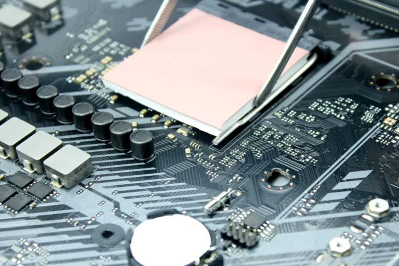
The most materials-intensive square centimeter in a test cell is the socket: the device under test is inserted thousands of times, contact pressure is set by springs and lids, and every re-landing refreshes the interface. Re-workability matters here as much as conductivity — a material that performs once but cannot survive re-insertion is the wrong material for test.
| Option | Typical bulk conductivity | Electrical | Re-workability | Best fit |
| Thermal grease | 1–5 W/m·K | Non-conductive (most) | Messy to refresh | Highest-performance single-use interfaces |
| Silicone Thermal pad / gap filler | 1–15 W/m·K | Non-conductive | Excellent — survives re-landing | Sockets, lids, gap-tolerant stack-ups; the test workhorse |
| Phase-change film | 3–8 W/m·K | Non-conductive | Good — re-wets each cycle | Thin, uniform, repeatable interfaces |
| Graphene Thermal sheet | 75–90 through-plane | Conductive | Excellent — survives re-landing | Sockets, lids, gap-tolerant stack-ups |
Overheating Chips? Improve Thermal Paths Quickly
Good semiconductor test equipment thermal design starts at tiny contact points where trapped air, uneven pressure, or material movement can send chip temperatures climbing fast. Better interfaces keep semiconductor test hardware cooler without making thermal design overly complicated.
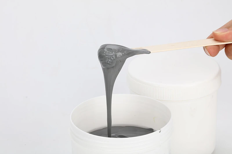
Applying Thermal Grease and Gap Filler Between Die and Heat Sink
In semiconductor test equipment thermal design, the path from semiconductor die to heat sink needs steady contact.
Interface control
- Apply a thin thermal interface material layer to support void elimination.
- Favor high thermal conductivity without excessive thickness.
Contact control
- Keep pressure even to lower interface resistance.
- Check coverage after assembly; small dry spots can hurt heat dissipation.
The basic idea is pretty simple: fill microscopic gaps, not the whole assembly.
Underfill Material for Enhanced Die Attach and Stress Relief
For high-power semiconductor test equipment thermal design, underfill can reinforce flip-chip connections while helping the thermal route.
- Match the polymer matrix and coefficient of thermal expansion to nearby materials.
- Control cure conditions around the die attach.
- Check mechanical stress under cyclic loading.
Good material matching improves long-term reliability and gives semiconductor thermal design a more stable operating base.
O-Ring and Gasket Sealing
Semiconductor test equipment thermal design also depends on keeping coolant and contact pressure where intended.
- Temperature resistance helps seals survive repeated hot runs.
- An elastomeric gasket supports pressure containment and limits fluid leakage.
- Controlling each air gap reduces unwanted thermal isolation.
- A well-compressed hermetic seal keeps the cooling path tight and predictable.
Semiconductor test equipment thermal design decides more than device temperature — it decides whether measurements can be trusted. Hot spots move parametrics, thermal cycling works interfaces loose, and every socket re-landing refreshes the contact on which the whole chain depends. The discipline is to sense first, size the architecture to heat density, and then sweat the materials: substrates, spreaders, interface films, and seals, multiplied across every test site.
Next step: share your DUT power map, socket or load-board geometry, and target junction-temperature window with Sheen’s engineering team for interface-material and silicone-foam sealing samples evaluated against your test conditions.
Sheen Thermal
Dongguan Sheen Electronic Technology Co., Ltd · Founded in 2008
Manufacturer of thermal interface materials and silicone foam for automotive electronics, energy storage, power electronics, communications and consumer electronics.
Certified
- ISO 9001:2015
- ISO 14001:2015
- IATF 16949:2016
What we supply
- Thermal conductivity Up to 90 W/m·K
- Thickness 0.3–10.0 mm
- Custom & samples Die-cut to drawing, 3–7 days
LAST:Nothing