
 English
 usheenthermal

Breakthrough Tech: The Ultra-thin Boron Nitride Thermal Conductive Layer (0.3mm)
Date:2026-08-10
Heat keeps wrecking compact electronics, boxing designers into bad trade-offs. The Ultra-thin boron nitride thermal conductive layer pad (0.3mm) cuts through that mess, moving heat fast while staying electrically insulating and slim enough to fit tight builds.
It holds steady under pressure, fits modern manufacturing, and solves overheating headaches across power, RF, and batteries.
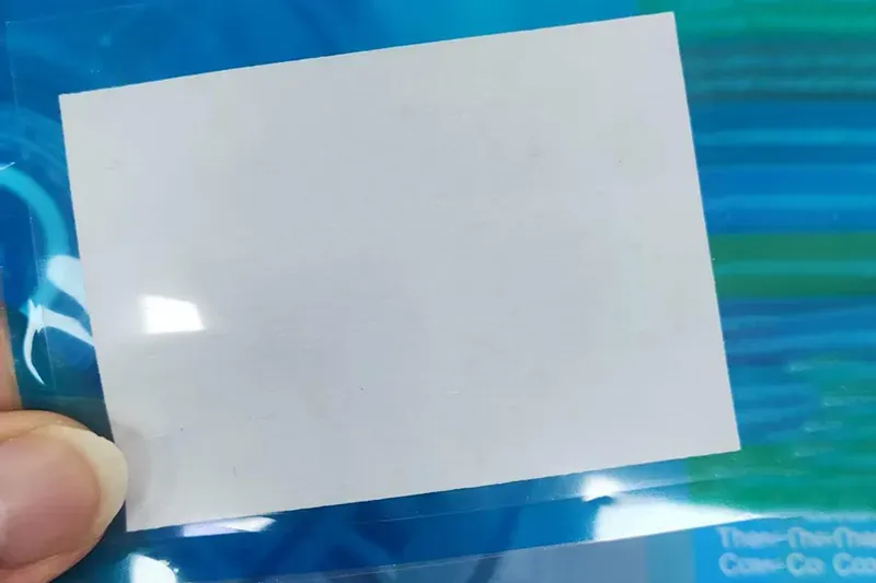
Reading Notes: Ultra-thin boron nitride thermal conductive layer (0.3mm) Essentials
-> Core Composition: Hexagonal BN composite laminated and sintered into a flexible, 0.3 mm film delivering high thermal conductivity and electrical insulation.
-> Thermal Performance: Rapid heat spreading prevents hotspots in power electronics, ICs, LEDs, and batteries under high–temperature stress.
-> Mechanical & Chemical Stability: Offers flexibility, chemical inertness, and resistance to oxidation, ensuring durability in compact and harsh environments.
-> Manufacturing & Integration: CVD/PVD deposition ensures uniform thickness, smooth surface, and strong adhesion for seamless integration into modern PCBs, RF modules, and 5G hardware.
hBN Thermal Conductive Layer: Material Science and Fabrication
The Ultra-thin boron nitride thermal conductive layer (0.3mm) is making heat control feel way less painful. By tuning boron nitride thin film into a flexible, reliable sheet, engineers now push compact devices harder without frying them. This boron nitride thermal layer balances strength, insulation, and heat flow in a surprisingly chill way.
From Boron Nitride Film to 0.3 mm Flexible Layer
Core transition of Boron Nitride:
- Film formation:Controlled thin film growth,Uniform 0.3 mm thickness targeting
- Structural tuning:Compression during lamination,Thermal bonding via sintering
Performance shaping:
- Mechanical side:Preserved mechanical flexibility,Crack resistance during bending
- Functional side:Stable dielectric behavior,Efficient heat transfer path
This is where the Ultra-thin boron nitride thermal conductive layer (0.3mm) turns from a fragile film into something you can actually use in tight electronics, especially with solutions refined by Sheen Technology.
How Hexagonal BN Composite Enables Superior Heat Spreading
A Hexagonal Boron Nitride network behaves like a highway for heat.
- Planar crystal layout → fast lateral conduction
- Composite material design → reduced thermal resistance
- Nanocomposite structure → bridges micro gaps
Key effects:
- Rapid heat spreading across chips
- Stable thermal conductivity under load
- Reliable thermal management in dense packaging
Data snapshot:
| Material Type | Thermal Conductivity (W/m·K) | Thickness (mm) | Heat Spread Rate | Electrical Insulation |
| h-BN Composite | 200–400 | 0.3 | High | Excellent |
| Aluminum | 205 | 1.0 | Medium | Poor |
| Graphite Sheet | 150–300 | 0.2 | High | Moderate |
| Silicone Pad | 1–15 | 0.5 | Low | Excellent |
| Copper | 385 | 1.0 | Medium | Poor |
The values for the hBN composites in the table represent the in-plane thermal conductivity of the hBN filler phase. For a 0.3 mm thick composite film, the effective through-plane thermal conductivity of the boron nitride thermal sheet supplied by Sheen reaches 16 W/m·K. Please contact Sheen Technology for ASTM D5470 test data regarding specific products.
Key Deposition Techniques for Uniform 0.3 mm Layers
- Start with deposition techniques selection
- Apply chemical vapor deposition for purity and alignment
- Use physical vapor deposition for surface precision
- Monitor layer thickness control in real time
- Finish with smoothing for consistent uniform layers
Quick notes:
- Better thin film fabrication = fewer defects
- Cleaner coating technology = stronger adhesion
- Even thickness = predictable cooling
The result is a stable Ultra-thin boron nitride thermal conductive layer (0.3mm) that performs the same across every inch—exactly what high-power electronics demand, and where Sheen Technology keeps pushing consistency forward.
5 Key Benefits Of A 0.3mm BN Layer
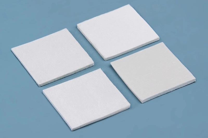
A Ultra-thin boron nitride thermal conductive layer (0.3mm) sounds technical, but in real-world electronics, it’s a quiet game-changer. From heat flow to signal clarity, this 0.3mm boron nitride layer keeps devices cool, stable, and efficient. If you’ve ever worried about overheating or miniaturization limits, this ultra-thin BN thermal layer steps in smoothly.
Lightning-Fast Thermal Conduction for High-Power Devices
Core effect of the Ultra-thin boron nitride thermal conductive layer (0.3mm):
Enhances thermal conductivity
- Moves heat away from chips fast
- Improves heat dissipation in compact builds
Supports high power devices
- Stabilizes thermal management
- Reduces hotspots in ICs
Flow of heat transfer optimization:
- Heat generated at source
- Rapid spread through ultra-thin BN thermal layer
- Efficient release into cooling systems
Short bursts: cooler chips. steadier output. better device performance.
Electrical Insulation Plus Mechanical Flexibility
Dual advantage stack:
Electrical side:
- Strong electrical insulation
- High dielectric strength
- Reliable insulating layer
Physical side:
- Excellent mechanical flexibility
- Works with flexible electronics
- Fits bendable substrates
The Ultra-thin boron nitride thermal conductive layer (0.3mm) keeps circuits protected while bending without cracking—pretty ideal for tight, modern layouts.
Chemical Inertness That Withstands High-Temperature Stress
Stability chain:
Built on chemical inertness
- Resists corrosion
- Limits material degradation
Handles high temperature stability
- Maintains thermal resistance
- Prevents oxidation resistance failure
Step-by-step durability:
- Exposure to heat
- No chemical breakdown
- Continued performance in harsh environments
This 0.3mm boron nitride layer doesn’t flinch under stress, which is exactly what power systems need.
Lightweight Dielectric Layer with Low Dielectric Constant
Quick breakdown:
- Lightweight material reduces load
- Acts as a clean dielectric layer
- Keeps low dielectric constant stable
Result chain:
- Better signal integrity
- Lower capacitance
- Easier miniaturization in electronic packaging
The ultra-thin BN thermal layer helps signals move cleanly without interference—small detail, big impact.
Unmatched Thickness Uniformity and Reliability Testing
Precision hierarchy:
- Consistent thickness uniformity
- Controlled via manufacturing precision
- Verified material reliability
Backed by strict testing protocols
- Adhesion checks
- Thermal cycling
- Long-term stress tests
Outcome:
- Stable performance consistency
- Extended device lifespan
- Trusted long-term stability
| Properties | Unit | SF1600-BN-03 | Test Method |
| Color | - | White | Visual |
| Thermal Conductivity | W/m·K | 16 | ASTM D5470 |
| Thermal Resistance (@40psi) | ℃*cm²/W | ≤0.3 | ASTM D5470 |
| Application temperature | ℃ | -40~150 | - |
| Thermal weight loss rate | % | ≤1 | - |
| Thickness | mm | 0.2~5.0 | ASTM D374 |
| Breakdown voltage | KV,@AC | ≥4 | ASTM D149 |
| Dielectric constant | F/m, @ 1MHz | ≤4.2 | ASTM D150 |
| Volume resistivity | Ω*cm, @250V | ≥10¹³ | ASTM D257 |
| Rebound rate | % | ≥90 | - |
| Density | g/cm³ | 1.6±0.2 | ASTM D792 |
| Hardness | shore 00 | 60~80 | ASTM D2240 |
| Flammability rating | - | V-0 | UL 94 |
With solutions from Sheen Technology, this Ultra-thin boron nitride thermal conductive layer (0.3mm) delivers repeatable quality that engineers can rely on without second-guessing.
Types Of Thermal Conductive Layers Explained
Thermal layers aren’t all built the same, and picking the wrong one can quietly wreck performance. From ultra-thin boron nitride thermal conductive layer (0.3mm) options to ceramics and TIMs, each material handles heat, electricity, and flexibility in its own way. Taking Sheen Technology’s products as an example:
| Material | Though-Plane K (W/m·K) | Dielectric (kV/mm) | Thickness (mm) | Best Application |
| 0.3mm BN pad | 16 | >12 | 0.2–5.0 | Dielectric heat spreading; 5G, power, LED, battery |
| Graphite Film | 5–30 | Conductive | 0.06–0.13 | High heat flux; no dielectric requirement |
| Graphene Sheet | 75–90 | Conductive | 0.3–2.0 | Experimental/niche; extreme lateral κ needed |
| Silicone TIM Pad | 1–15 | >6 | 0.3–10.0 | Gap filling; compressibility needed |
Boron Nitride Sheet vs. Graphite Film
- Boron nitride sheets act as a quiet achiever: solid thermal conductivity, strong electrical insulation, and stable heat dissipation in tight electronics.
- Graphite film pushes higher heat flow but sacrifices dielectric safety.
Material behavior
- BN sheet → balanced material properties, safe for circuits
- Graphite layer → faster lateral heat spread, but conductive
Application logic
- Use BN when insulation matters
- Use graphite when raw cooling dominates
At Sheen Technology, these BN layers are tuned for devices where both safety and cooling can’t be compromised.
Graphene Sheet: Ultra-thin Carbon Alternative
Graphene is basically the extreme version of carbon sheets,Ultra-thin boron nitride thermal conductive layer vs graphene sheet often comes down to conductivity vs insulation
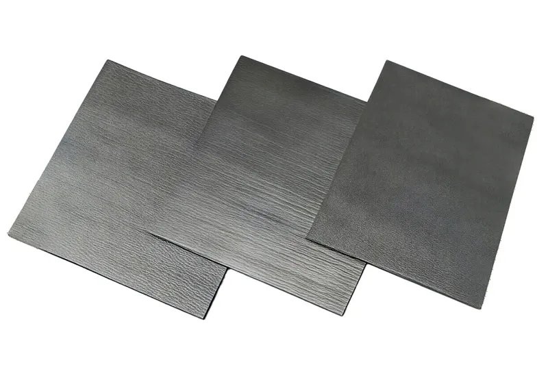
Key contrasts
- Graphene: unmatched heat transfer, but electrically active
- BN alternative: slightly lower performance, far safer
“Advanced carbon materials continue to push thermal limits, but insulation constraints still shape adoption in consumer electronics” — IDTechEx, 2025
Ceramic Substrate: Aluminum Nitride and Silicon Carbide
Core materials
Ceramic substrate options include:
- Aluminum nitride → strong thermal management, good insulation
- Silicon carbide → extreme high temperature endurance
Structural traits
- Thicker than ultra-thin boron nitride thermal conductive layer (0.3mm)
- Rigid, not flexible like a sheet
Use cases
- Power electronics
- Harsh environments needing a heat spreader
In contrast, Sheen Technology keeps things slimmer with ultra-thin BN solutions where space is tight.
Thermal Interface Materials (TIMs) Overview
Thermal interface materials fill microscopic gaps
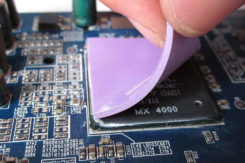
Common forms:
- thermal grease
- thermal pad
- thermal paste
Step-by-step heat path:
- Surface contact forms
- Air gaps increase thermal resistance
- TIMs act as a gap filler
- Heat flows more smoothly
Still, TIMs lack the structure of a ultra-thin boron nitride thermal conductive layer (0.3mm) or a solid BN layer.
Quick comparison:
- TIMs = flexible, easy, but temporary feel
- BN sheets = stable, uniform, long-term
Need thermal conductivity, dielectric strength, thickness tolerance, breakdown voltage, and thermal cycling data for ultra-thin boron nitride thermal conductive layers? Download the product datasheets to compare 0.3mm BN sheets, graphite films, graphene alternatives, and ceramic substrates for power electronics, 5G base stations, LED modules, and battery thermal management.
Thin Vs. Thick: Thermal Layer Showdown
A quick, real-world look at how heat actually moves in tight electronics. The Ultra-thin boron nitride thermal conductive layer (0.3mm) shows up everywhere from compact modules to dense boards, while thick ceramics still hold ground in rugged builds. Here’s how Boron Nitride tech stacks against classic Ceramic approaches without the fluff.
Ultra-thin 0.3 mm BN Sheet
The Ultra-thin boron nitride thermal conductive layer (0.3mm) keeps things light and fast, pushing thermal conductivity where it counts. With 0.3mm thickness, it slips into cramped layouts and still spreads heat across each layer efficiently. Core behavior
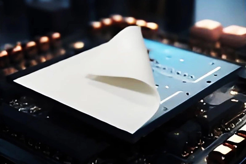
Heat path design
- In-plane spreading (dominant):Uses Boron Nitride platelets to guide heat laterally,Reduces hotspots under chips in high-density layouts
- Through-thickness transfer:Short path due to ultra-thin profile,Works best with flat contact and light pressure
Mechanical traits
- Flexibility:Conforms to uneven surfaces,Supports bendable assemblies
- Weight:Minimal mass improves mobile devices
Integration in material science workflows
- Lamination:Pairs with adhesives or tapes
- Direct interface:Acts as a heat dissipation layer between IC and sink
The Ultra-thin boron nitride thermal conductive layer (0.3mm) also trims stack height, a win for miniaturization.
At scale, the Ultra-thin boron nitride thermal conductive layer (0.3mm) aligns with advanced technology trends—denser boards, tighter envelopes, cooler chips.
Traditional Thick Ceramic Substrate
Thick ceramic substrate options lean on durability and stable heat transfer, but they trade off size and flexibility. The Ultra-thin boron nitride thermal conductive layer (0.3mm) often replaces them where space is tight, though ceramics still shine in harsh settings. Performance stack
Thermal management
- High-temperature tolerance in traditional material systems,Predictable behavior under load
- Interface limits,Thicker path increases resistance vs thin BN layer
Mechanical profile
- Rigidity:Strong, but limits design freedom
- Weight:Heavier assemblies affect portability
Use in electronic packaging
- Power modules,Good for high heat and structural needs
- Legacy designs,Easier drop-in for existing tooling
Quick compare:
1) Size: thick vs the Ultra-thin boron nitride thermal conductive layer (0.3mm)
2) Flex: rigid vs conformable BN sheet
3) Heat spread: bulk vs lateral spreading
Sheen Technology brings the thin route into practical builds, where the Ultra-thin boron nitride thermal conductive layer (0.3mm) keeps temps down without bulking things up.
Struggling With Hotspots? Try BN Layer
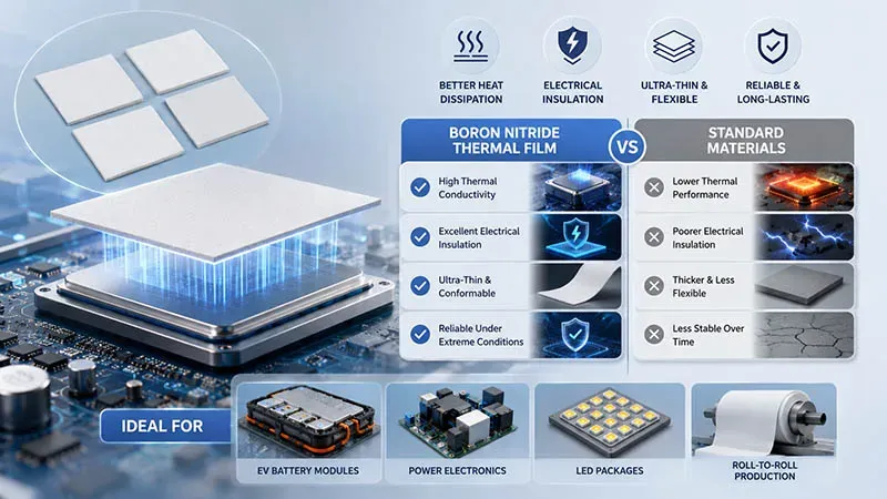
Hotspots can sneak up fast in modern electronics, especially when power density climbs. A slim fix is gaining traction: the Ultra-thin boron nitride thermal conductive layer (0.3mm). Split it up—ultra-thin BN layer, boron nitride thermal sheet, 0.3mm thermal layer—and you’ll see how flexible it gets across designs.
Hotspot Mitigation in Power Electronics with BN Composite
Core path to Hotspot mitigation in Power electronics using BN composite:
Heat spread
- Interface: ultra-thin BN layer sits between chip and sink
- Lateral flow: boron nitride thermal sheet evens gradients
Device stability
- Lower peak temps in Semiconductors
- Reduced drift in Electronic devices
System gains
- Cleaner Thermal management loop
- Faster Heat dissipation
Integration sequence
1) Map hotspots via IR scan
2) Apply 0.3mm thermal layer with light pressure
3) Validate delta-T and cycling
Practical notes
- Works with TIM stacks; pairs well with Sheen Technology materials
- Keep surfaces flat; avoid air gaps
Hot zones shrink. Power headroom grows. The Ultra-thin boron nitride thermal conductive layer (0.3mm) keeps temps even without bulk.
Boosting LED Module Lifespan via 0.3 mm Thermal Management
LEDs hate heat spikes. A boron nitride thermal sheet under the board drops junction temps and steadies output. The Ultra-thin boron nitride thermal conductive layer (0.3mm) acts like a quiet equalizer—thin, quick, reliable for LED module builds and Reliability goals.
What improves
- Lifespan extension and lumen stability
- Efficient Heat transfer through a 0.3mm layer
- Consistent Thermal management with Boron nitride
Quick workflow
1) Clean substrate
2) Place ultra-thin BN layer
3) Clamp and reflow-check
Measured impact
| Configuration | Junction Temp (°C) | L70 Life (hrs) | Thermal Resistance (°C/W) |
| No BN layer | 118 | 18,000 | 2.6 |
| 0.3mm thermal layer | 101 | 28,500 | 1.9 |
| Ultra-thin BN layer (optimized) | 96 | 34,200 | 1.6 |
Sheen Technology supplies consistent thickness control, so the 0.3mm thermal layer performs the same across batches.
Battery Thermal Management Enhanced by Flexible BN Film
For Battery thermal management in Energy storage:
Flexible stack
- Wrap cells with flexible BN film,Route heat to cold plates for tight Heat control
- Higher Thermal conductivity lowers gradients,Better Battery performance and cycle life
EV context
- Stable packs for Electric vehicles under fast charge
- Multi-step rollout:Cell mapping → Film placement (ultra-thin BN layer) → Compression set → BMS tuning → Cycle test
Field cues
- Fewer hotspots, tighter ΔT, safer fast charging
- Ultra-thin boron nitride thermal conductive layer (0.3mm) fits narrow gaps
“Thermally conductive, electrically insulating films are becoming standard in EV packs to control cell-to-cell gradients and extend cycle life,” notes a 2025 IDC energy storage brief.
Sheen Technology options include flexible boron nitride thermal sheets tailored to pack geometry, keeping that 0.3mm thermal layer effective where space is tight.
Application Scenarios: 0.3mm BN In 5G Base Stations
Ultra-thin boron nitride thermal conductive layer (0.3mm) is quietly doing heavy lifting inside modern 5G gear. From packed PCB line cards to antenna modules, this ultra-thin BN layer keeps heat under control while protecting signal quality. It’s a small material tweak with a big system-level payoff, especially when density keeps climbing.
Thermal Management for High-Frequency PCB Line Cards
Within thermal management of high-frequency PCB line cards, the ultra-thin boron nitride thermal conductive layer (0.3mm) works like a hidden heat highway.
Core function stack
Heat spreading via boron nitride
- reduces hotspots in dense routing zones
- stabilizes impedance under thermal drift
Interface efficiency
- ultra-thin BN layer fits tight gaps
- improves contact across stacked materials
Deployment flow
- Integrate Ultra-thin boron nitride thermal conductive layer (0.3mm) beneath active regions
- Align with heat dissipation paths toward chassis
- Maintain signal integrity during sustained 5G load
Outcome tiers
- Device level: cooler traces
- Board level: fewer failures
- System level: stronger 5G base stations uptime
Sheen Technology applies this ultra-thin boron nitride sheet approach to keep boards stable without adding bulk.
Heat Dissipation in Integrated Circuit Power Amplifiers
In integrated circuits and power amplifiers, heat spikes fast, and cooling lag hurts performance.
• Ultra-thin boron nitride thermal conductive layer (0.3mm) improves thermal conductivity at the chip interface
• Acts as a thermal interface between die and package
• Supports long-term reliability in semiconductor devices used in 5G infrastructure
“Advanced thermal interface materials are becoming critical to sustaining RF output stability in next-generation base stations.” — 2025 industry analysis, Yole Group
Sheen Technology integrates ultra-thin BN layer solutions that balance thinness and durability, avoiding the trade-off engineers used to accept.
Reliable Dielectric Layer for Antenna Module Performance
5G mMIMO antenna arrays concentrate 64–128 transceiver chains in a single panel, generating 500–1,000W total dissipation. The 0.3mm BN layer's combination of lateral heat spreading and low dielectric constant (Dk ~3–4, Df ~0.001–0.003 at 3.5 GHz) makes it suitable for direct integration beneath antenna patch elements.
The Ultra-thin boron nitride thermal conductive layer (0.3mm) doubles as a dielectric layer in compact antenna modules.
- Low dielectric constant helps preserve signal integrity.
- Stable under radio frequency stress.
- Strong thermal stability keeps performance consistent.
- Better electromagnetic performance without extra thickness.
In tight 5G communication hardware, this thin boron nitride layer quietly keeps both heat and signals in check.
【Request a Custom Quote】Not sure whether a 0.3mm BN sheet, graphite film, or ceramic substrate is the best thermal conductive layer for your application? Send us your thermal conductivity target, operating temperature range, dielectric requirements, thickness constraints, and mechanical flexibility needs, and our engineers can recommend the right solution for your project.
Sheen Thermal
Dongguan Sheen Electronic Technology Co., Ltd · Founded in 2008
Manufacturer of thermal interface materials and silicone foam for automotive electronics, energy storage, power electronics, communications and consumer electronics.
Certified
- ISO 9001:2015
- ISO 14001:2015
- IATF 16949:2016
What we supply
- Thermal conductivity Up to 90 W/m·K
- Thickness 0.3–10.0 mm
- Custom & samples Die-cut to drawing, 3–7 days