
 English
 usheenthermal

Why Does the Space Between Your Heatsink and Chip Need a Thermal Silicone Pad?
Date:2026-10-31
The heatsink is installed. So why is that one component on the board still running hot? In designs where multiple VRAM chips or power components share a single cooling structure, one easily overlooked culprit is this: the contact between component and heatsink isn’t as complete or stable as you think.
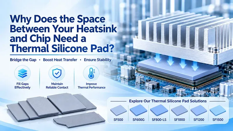
Components sit at different heights. PCBs and metal parts all carry tolerances. A heatsink that looks perfectly seated may not actually touch every heat-generating surface. For spots that need an assembly gap bridged, a thermal silicone pad with the right thickness and mechanical properties helps move heat from the component to the heatsink, cold plate, or metal chassis.
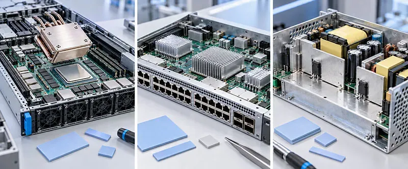
Figure 1. Application concept image for servers, switches, and industrial power supplies — AI-generated illustration, not a customer installation photo.
Its value goes well beyond one conductivity number. Whether it fills the gap, conforms to surfaces, and lets components keep working under tolerable loads — that’s what decides if the material does its job in your device.
This article starts from real component locations in common equipment, walks through what thermal silicone pads do, where they apply, and where the technology is heading — then uses six Sheen products (SF500, SF600G, SF800-LS, SF1000, SF1200, SF1500) to show how to build a sample list worth testing.
Where These Devices Can Use Thermal Silicone Pads
Thermal silicone pads belong to the thermal interface material (TIM) family. They typically arrive as sheets or die-cut parts assembled between a heat-generating component and a cooling part — a natural fit for structures that need gap filling, tolerance compensation, and pre-formed placement. Applications are broad; which interface to use one on depends on the heat path.
| Application Area | Possible Gap-Filling Locations | What Engineers Want to Solve |
| Computing & storage | Servers, accelerator cards, VRAM, power delivery zones, SSDs | Stable contact between multiple components and the cooling structure |
| Networking & telecom | Switches, routers, PHY and control ICs in base stations | Connect scattered heat sources to local heatsinks or metal lids |
| Power & industrial control | Heat spots on power boards, driver boards, control boards | Use baseplates or chassis for heat transfer while meeting assembly and insulation needs |
| Consumer electronics | PCs, graphics cards, gaming devices, smart terminals | Compensate height differences and assembly gaps in compact structures |
| Automotive electronics | Vehicle control units, navigation, some power boards | Handle structural tolerances and maintain contact after thermal cycling |
| LED & display equipment | Lamp drivers, control boards, matching thermal interfaces | Link heat sources to cooling parts with easy pre-formed assembly |
This table describes application directions for the material category — it does not mean the six SF products have completed certification or platform validation for every scenario. High-voltage isolation, optical contamination sensitivity, and automotive long-term reliability must be confirmed project by project.
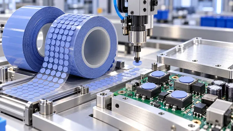
Figure 2.SHEEN pre-formed die-cut pads, actual product photo. Supply format and specific product specs to be confirmed separately.
Which Structures Deserve Pre-Formed Pads First
Three conditions make the case. First, a defined gap exists between component and heatsink that a material must bridge. Second, multiple components at different heights need a compliant material to improve contact. Third, production wants positionable, pre-formed parts — cutting out on-site mixing or dispense-volume control.
These conditions explain why thermal silicone pads so often show up near VRAM, power delivery, and control components. A pad is part of the thermal design, but it also touches die-cut dimensions, placement location, liner peeling, and rework operations.
Fill the Gap and Conform — Only Then Does Heat Flow Well
When two solid surfaces meet, microscopically only part of the area truly touches; the rest can trap air. Thermal silicone pads use a deformable silicone matrix loaded with thermally conductive filler to fill that interface under proper assembly conditions, improving thermal coupling between heat source and cooling part.
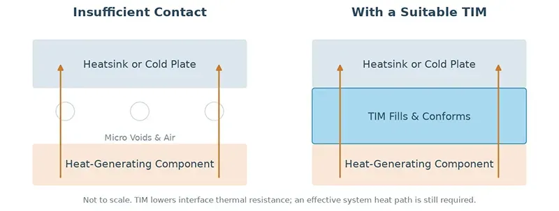
Figure 3. Interface filling and heat flow path — structure not drawn to scale.
Evaluate three conditions together when selecting:
| Condition | What It Affects | The Question to Ask |
| Thermal conductivity | Bulk heat-transfer capability of the material | At the target thickness, does bulk resistance meet the thermal budget? |
| Effective thickness & conformity | Heat-transfer distance and contact state on both sides | Does contact form at both minimum and maximum gap? |
| Compression force & structure | Loads on components, solder joints, PCB, and fasteners | Can the structure survive the compression needed for conformity? |
For example: a high-conductivity material that’s too thick can still carry excessive bulk resistance, and a pad that can’t compress to the needed thickness within the allowable load may compromise contact. Flip it around — chasing softness while ignoring the thermal budget doesn’t finish the job either. Engineers need a combination where thermal performance and mechanical conditions match.
That’s exactly why the SHEEN SF series spans multiple conductivity grades and specs: on the same board, different zones can use different materials based on heat load, gap, and load. For thin interfaces or main-chip contact surfaces, also evaluate grease, phase-change materials, gels, and other TIM forms.
What Design Changes Shape the Future of Thermal Silicone Pads
The application outlook should be judged by what device designs now demand from the interface. High-density computing, compact structures, and volume-production reliability are pushing material selection beyond conductivity grades into complete assembly behavior.
High-Density Computing Puts Local Heat Paths in the Spotlight
NVIDIA’s DSX documentation frames compute, power delivery, direct liquid cooling, and system efficiency in one design framework; data center material literature likewise lists high heat density and thermo-mechanical reliability as central topics. [9–10] For board-level design, this means VRAM, power delivery, and control components beyond the main chip all need their heat paths confirmed against the actual structure.
Liquid Cooling Still Needs a Device-to-Cold-Plate Interface Design
Liquid cooling moves heat differently than air, but component surfaces still need effective thermal coupling to the cold plate. Our engineering judgment: interface thickness, contact state, and assembly load still shape the choice. Whether a given location calls for a pad, gel, phase-change material, or another TIM comes down to structural and reliability requirements.
Material Performance Must Match Assembly and the Full Service Cycle
For devices where many components share a cooling structure, the selection value of a soft material lies in whether it achieves contact within an acceptable load. Formal adoption also means checking die-cutting and placement, post-compression retention, and performance after thermal cycling. One initial temperature test answers only part of the validation question.
| Direction Worth Watching | Interface Requirement | Implication for SF Series Selection |
| Localized high-heat-flux zones | Lower interface resistance within allowable thickness | Evaluate SF1000, SF1200, or SF1500 |
| Load-limited multi-component structures | Full contact within allowable load | Add SF800-LS as a comparison sample |
| Multi-model, volume assembly | Dimensions, positioning, thickness, process stability | Confirm actual die-cut and delivery structure |
Sheen’s position on selection direction: center on interface thermal resistance under real assembly conditions, while evaluating mechanical load and long-term contact behavior. This describes a technical trend — it does not equate industry change with sales growth of any pad, nor does it imply certification for specific chip platforms.
Server VRAM and Power Delivery: Every Component Needs Real Contact
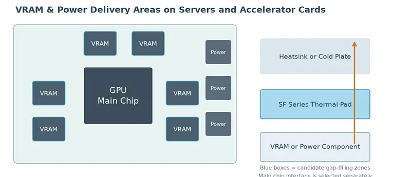
Figure 4. Server and accelerator card application schematic — blue boxes mark candidate gap-filling zones.
Picture an accelerator card: the main chip, surrounding VRAM, and power components share part of the cooling structure, but their heights aren’t identical. Once the heatsink is seated, some locations contact fully while others may still hold a gap. (This scenario illustrates selection logic — it is not a Sheen customer test case.)
If the main problem is limited assembly force, put SF800-LS on the sample list first. Its design point combines an 8 W/(m·K) grade with a soft character — a natural candidate for evaluation around sensitive components, board flex, and clamp loads. What to verify: within the component’s allowable load and fixed assembly gap, can the material achieve fuller contact and more stable temperatures?
If the main problem is a tighter thermal budget, compare SF600G, SF1000, and SF1200; if the design accepts incoming nominal thicknesses from 1 mm up, add SF1500 to the candidates. Keep the same board, cooling structure, and thermal boundaries — and record assembly loads — so you can judge what the material swap actually bought you.
The main interface of a GPU, CPU, ASIC, or HBM package needs its own material selection based on its thickness and load conditions. Surrounding gap-filling pads should also avoid being so thick that they interfere with seating the main heatsink.
For projects like these, what’s worth requesting is not an isolated highest-conductivity grade, but a set of comparison samples designed around your existing gaps, loads, and temperature targets.
Why SF800-LS Belongs on Low-Load Sample Lists
The case for SF800-LS is straightforward: when assembly load limits pad compression and interface conformity, it offers a candidate that takes both conductivity and compliance seriously. Whether it fits your board is something the actual structure can answer.
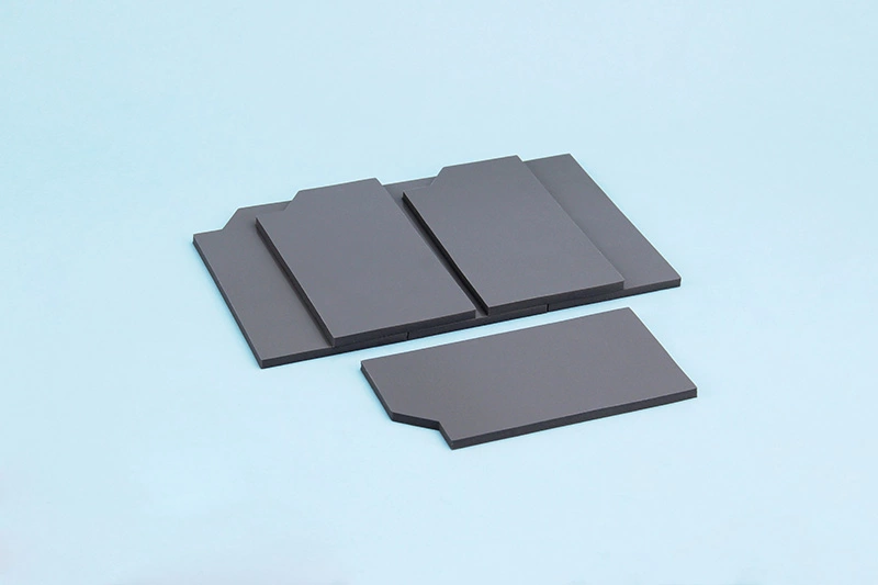
Figure 5. SF800-LS product image from the official datasheet.
| Datasheet Item | SF800-LS Value | How to Read It |
| Thermal conductivity | 8 W/(m·K) | Base material value, excluding auxiliary layers, as noted in the datasheet |
| Hardness | Shore 00 25, 30-second reading | Softness under specified test conditions |
| Nominal thickness | 1–5 mm | Match to structural gap and tolerances first |
| Application temperature | −40 to 125 °C | Long-term service conditions validated per project |
| Compression force under specified conditions | ≤150 N | Specimen area and compression conditions shown below |
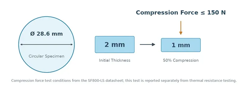
Figure 6. SF800-LS compression force test conditions — 2 mm circular specimen, 28.6 mm diameter, 50% compression.
≤150 N is a force value under those specific conditions — you cannot treat it as the assembly force for a pad of any size. It is also a separate test from thermal resistance measurement, and 50% is not a recommended compression rate for every project. Actual selection needs the target compression range, allowable component load, and the corresponding force-displacement data.
Write the SF800-LS sample objective down explicitly: within the existing structure and allowable load, verify contact imprint, hot-spot temperature, and reassembly consistency. Now 8 W/(m·K) and the soft design have something concrete to be judged against.
Switches and Telecom Equipment: Connect Scattered Heat Sources to the Cooling Structure
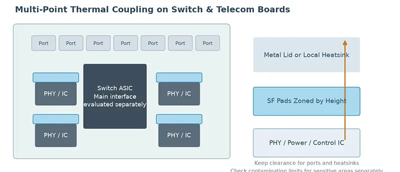
Figure 7. Switch and telecom board application schematic — main chip and surrounding ICs evaluated as separate zones.
Heat sources on switch and telecom boards can include the switch ASIC, PHYs, processors, power stages, and control ICs. Local heatsinks, metal lids, and airflow ducts together define the heat path. Thermal silicone pads can fill the gaps between suitable components and cooling structures, giving scattered heat sources a usable thermal connection.
Pick Candidates by Height Difference and Assembly Force
For routine peripheral component gap filling, SF600G is the 6 W/(m·K) candidate. Where lid clamping force, PCB flex, or component load is the binding constraint, evaluate SF800-LS first. For tighter thermal budgets, then compare SF1000, SF1200, or SF1500.
Elongated or large-area coverage structures especially need a check of total assembly force, fastener positions, and component height differences. Zoned thicknesses or die-cut shapes are a legitimate engineering direction — the final structure gets decided by assembly and temperature testing together.
Connectors and Optically Sensitive Areas Need Project-Specific Requirements
Different zones of telecom equipment can have different material compatibility requirements. SF800-LS is a silicone-based thermal pad; its documentation cannot be used to presume silicone-free, zero oil-bleed, or zero volatiles. Near optical windows, contacts, or connectors, define contamination limits and check the corresponding reports. Projects requiring non-silicone materials should evaluate an explicitly non-silicone system.
For these projects, the sample comparison should focus on whether every component makes contact, whether the lid seats stably, and the temperature spread after repeated assembly. Those tell you far more about whether a solution will land reliably than one temperature reading on one chip.
Power and Industrial Control: Put the Chassis and Baseplate to Work
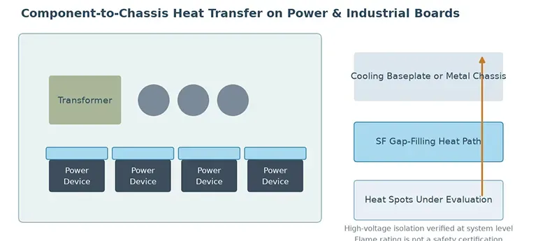
Figure 8. Power and industrial control application schematic — specific insulation structures require separate design and validation.
For suitable power, driver, and control boards, a cooling baseplate or metal chassis can become part of the heat path. Thermal silicone pads fill the gap between heat spots and cooling structures — letting designers use existing metal for heat transfer and enabling pre-formed assembly to drawing.
Start Routine Gap Filling with SF500
SF500 offers a 3 W/(m·K) grade and a 0.5–10 mm nominal thickness range — a candidate for looser thermal budgets or locations needing thicker gap compensation. SF600G brings 6 W/(m·K); for more concentrated heat flow where structure allows, keep comparing SF1000, SF1200, or SF1500.
When Control ICs or Thin Boards Are Load-Limited, Consider SF800-LS
If pressure conformity is limited by component or board strength, add SF800-LS to the comparison. What needs verifying is whether stable contact forms under the given mounting conditions. The real effect of a soft material should be evaluated together with die-cut area, stop structures, and thermal testing.
Heat Path and Electrical Isolation Are Separate Checkboxes
All six datasheets list electrical insulation and flame-related parameters. SF500 lists breakdown voltage ≥6 kV; the other five in this article list ≥4 kV — all under AC, 1 mm conditions. That is not an allowable continuous working voltage. High-voltage isolation still requires checking thickness, edge distances, environment, and aging against system-level standards.
SF500’s application temperature is −40 to 150 °C; the other five are −40 to 125 °C. The upper limit is not a proxy for long-term life. Power and industrial projects should fold thermal cycling, damp heat, vibration, and other real conditions into validation.
How the Six SF Products Form a Clear Selection Ladder
First decide whether the constraint comes from thermal budget, gap, or assembly force — then look at specific grades. The table below uses currently confirmed official datasheets; SF500 uses only the standard SF500 column, and the 8 W/(m·K) tier uses the standalone SF800-LS documentation.
| Grade | Conductivity W/(m·K) | Thickness mm | Hardness Shore 00 | Needs to Evaluate First |
| SF500 | 3 | 0.5–10 | 35–90 | Routine gap filling; wide thickness range |
| SF600G | 6 | 0.5–5 | 35–90 | Stepping up conductivity from routine gap filling |
| SF800-LS | 8 | 1–5 | 25¹ | Load-limited assembly needing compliant conformity |
| SF1000 | 10 | 0.5–5 | 35–90 | Tighter interface thermal budgets |
| SF1200 | 12 | 0.5–5 | 35–90 | Further conductivity grade increase |
| SF1500 | 15 | 1–5 | 35–90 | High-conductivity gap filling where structure allows |
SF800-LS is a 30-second hardness reading; other grades list selectable hardness ranges without noting the same reading timing. When choosing a specific softness grade, confirm it against delivery specs and test conditions.
Area-normalized resistance must be read together with specimen thickness and pressure:
| Grade | Area Resistance °C·in²/W | Specimen Thickness (Datasheet) | Test Conditions |
| SF500 | ≤0.44 | 1 mm | 50 psi, ASTM D5470 |
| SF600G | ≤0.24 | 1 mm | 50 psi, ASTM D5470 |
| SF800-LS | 0.07 | 2 mm | 50 psi, ASTM D5470 |
| SF1000 | ≤0.13 | 1 mm | 50 psi, ASTM D5470 |
| SF1200 | ≤0.11 | 1 mm | 50 psi, ASTM D5470 |
| SF1500 | ≤0.07 | 1 mm | 50 psi, ASTM D5470 |
SF800-LS was tested at a different specimen thickness — don’t rank the grades on these numbers alone. 50 psi ≈ 345 kPa is a test pressure; if your real structure differs, get data under matching conditions and validate. Nor should the datasheet’s specimen thickness be casually reinterpreted as the effective post-compression thickness.
All six datasheets list UL94 V-0 and PASS items for RoHS, Halogen, and REACH. Sheet format is 200 × 300 mm or custom, with die-cut shapes available for evaluation. At project adoption, verify reports and delivery requirements against the specific grade, thickness, adhesive backing, or reinforcement layer structure.
After Requesting Samples, Validate One Concrete Improvement Goal
A worthwhile sample test starts from the limitation of your current solution. If the problem is load-limited contact, compare contact and temperature within the allowable load. If the problem is the thermal budget, fix the structural boundaries and compare thermal behavior. The framework below is a suggested validation approach — not existing Sheen customer test results.
| Current Problem | Sample Combination to Discuss | Key Records |
| Limited assembly force, insufficient contact | Current material vs. SF800-LS | Actual load, compressed thickness, contact imprint, hot-spot temperature |
| Thermal budget needs further improvement | Screen among SF600G, SF1000, SF1200 | Temperatures and assembly state with structure and thermal boundaries fixed |
| Evaluating a higher conductivity grade | Add SF1500 where structure allows | Effective thickness, load, initial and post-aging thermal behavior |
Why Sample Thickness Deserves Just as Much Attention
Under a uniform 1D heat-flow model, bulk thermal resistance is R = t / (kA) — where t is effective compressed thickness, k is conductivity, and A is heat-transfer area. The real interface also includes contact resistance on both sides.
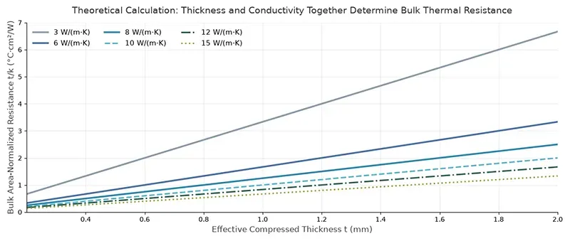
Figure 9. Theoretical effect of thickness and conductivity on bulk area-normalized resistance — contact resistance not included.
Example: at 1 mm effective thickness, 20 × 20 mm transfer area, and 10 W crossing the interface, a material at k = 8 W/(m·K) gives bulk resistance of about 0.313 K/W and a corresponding temperature difference of about 3.13 °C. That is a calculation example, not a measured temperature drop for SF800-LS — but it shows why thickness, area, and conductivity grade must be read together.
After the initial comparison, run reassembly, thermal cycling, or other reliability tests per your project. Watch temperatures, contact, and load together — that’s how sample results turn into a usable delivery specification.
From Learning About Materials to One Effective Sample Conversation
1. Can I ask for advice if I don’t know which grade to pick?
Yes — start by describing the device and the heat-generating locations, plus the approximate gap and the area to cover. Power, allowable load, and target temperatures can be added in later technical discussion to progressively narrow the candidates.
2. Is SF800-LS suitable for every low-resistance interface?
It’s mainly worth evaluating in gap-filling structures where assembly load is limited and the 1–5 mm nominal thickness range fits. Main-chip thin interfaces or incoming specs below 1 mm need a separate material and structure discussion. For detailed information and applications regarding the SF800-LS, please visit this link: https://www.sheenthermal.com/low-stress-thermal-pad-selection-guide.html
3. What if I have optical contamination or non-silicone requirements?
Define the contamination limits and test methods first. SF800-LS is a silicone-based pad — nothing about its suffix implies non-silicone or zero volatiles. If non-silicone is required, the conversation should move to an explicitly non-silicone material system.
4. What other documentation should I ask for with samples?
Beyond the datasheet, ask — as your project needs — for thermal resistance near your target pressure, compression force-displacement curves, and reliability data. Whether reports cover your target grade, thickness, and structure should be confirmed item by item in technical discussion.
Let SHEEN Start from Your Actual Interface
Three pieces of information are enough for a first conversation: what device and location it’s for, roughly how thick the gap is, and how large the pad needs to be. If you have the current material or structural drawings, send those too. Sample specs, quantities, and delivery arrangements get confirmed in discussion.
If your VRAM or power delivery structure is limited by assembly load, say so directly: you’d like to evaluate SF800-LS against your current material, comparing contact and temperature under the same structure.
Selection consulting & sample requests — SHEEN official contact
Sheen Thermal
Dongguan Sheen Electronic Technology Co., Ltd · Founded in 2008
Manufacturer of thermal interface materials and silicone foam for automotive electronics, energy storage, power electronics, communications and consumer electronics.
Certified
- ISO 9001:2015
- ISO 14001:2015
- IATF 16949:2016
What we supply
- Thermal conductivity Up to 90 W/m·K
- Thickness 0.3–10.0 mm
- Custom & samples Die-cut to drawing, 3–7 days
LAST:Nothing