
 English
 usheenthermal

Boron Nitride Thermal Pads for Electrically Insulating Optical Module Designs
Date:2026-09-09
Heat is squeezing optical modules from every corner, while conductive housings make electrical isolation a must-have. Boron Nitride Thermal Pads for Optical Module designs tackle that tightrope with heat transfer, dielectric protection, and compliant contact in one practical interface.
For volume buyers, specs go beyond W/m·K: thickness, compression, dielectric strength, precision, consistency, and compliance.
Reading Notes: Boron Nitride Thermal Pads for Optical Module
➔ Material Blend: Hexagonal boron nitride in a silicone elastomer matrix ensures high thermal conductivity and electrical insulation.
➔ Thermal Performance: Optimized filler loading reduces interface impedance, efficiently transferring heat from laser diodes to housings.
➔ Mechanical Fit: Precise pad thickness, die-cut dimensions, and controlled compression deliver reliable contact without excess stress.
➔ Electrical Safety: High dielectric breakdown strength and volume resistivity prevent shorts between optoelectronics and conductive chassis.
➔ Quality & Compliance: RoHS-certified pads with defined shelf life and storage conditions maintain consistent performance in data-center optics.
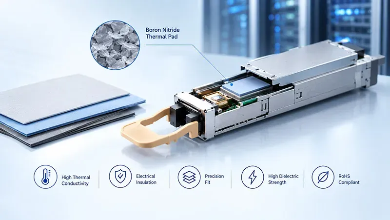
Note: This diagram was created with AI assistance and is not an actual photograph; the illustrated structure and operational logic align with real-world engineering applications and serve as a valid reference.
Key Properties Of Boron Nitride Thermal Pads
Boron Nitride Thermal Pads for Optical Module designs must move heat, protect circuits, and fit tight spaces. Sheen Technology combines these practical needs so optical module cooling stays manageable.
Sheen Technology Boron Nitride Thermal pad performance properties:
| Properties | Unit | SF1600- BN-03 | SF1600-BN-05 | SF1600-BN-07 | SF1600-BN-10 | SF1600-BN-15 | SF1600-BN-20 | SF1600-BN-30 | Test Method |
| Color | - | White | White | White | White | White | White | White | Visual |
| Thermal Conductivity | W/m·K | 16 | 16 | 16 | 16 | 16 | 16 | 16 | ASTM D5470 |
Thermal Resistance (@40psi) | ℃*cm²/W | ≤0.3 | ≤0.5 | ≤0.7 | ≤0.8 | ≤1.1 | ≤1.4 | ≤1.7 | ASTM D5470 |
Application temperature | ℃ | -40~150 | -40~150 | -40~150 | -40~150 | -40~150 | -40~150 | -40~150 | - |
Thermal weight loss rate | % | ≤1 | ≤1 | ≤1 | ≤1 | ≤1 | ≤1 | ≤1 | - |
| Thickness | mm | 0.2~5.0 | 0.2~5.0 | 0.2~5.0 | 0.2~5.0 | 0.2~5.0 | 0.2~5.0 | 0.2~5.0 | ASTM D374 |
| Breakdown voltage | KV,@AC | ≥4 | ≥5 | ≥6 | ≥10 | ≥12 | ≥12 | ≥12 | ASTM D149 |
| Dielectric constant | F/m, @ 1MHz | ≤4.2 | ≤4.2 | ≤4.2 | ≤4.2 | ≤4.2 | ≤4.2 | ≤4.2 | ASTM D150 |
| Volume resistivity | Ω*cm, @250V | ≥10¹³ | ≥10¹³ | ≥10¹³ | ≥10¹³ | ≥10¹³ | ≥10¹³ | ≥10¹³ | ASTM D257 |
| Rebound rate | % | ≥90 | ≥80 | ≥70 | ≥70 | ≥60 | ≥60 | ≥60 | - |
| Density | g/cm³ | 1.6±0.2 | 1.6±0.2 | 1.6±0.2 | 1.6±0.2 | 1.6±0.2 | 1.6±0.2 | 1.6±0.2 | ASTM D792 |
| Hardness | shore 00 | 60~80 | 60~80 | 60~80 | 60~80 | 60~80 | 60~80 | 60~80 | ASTM D2240 |
| Flammability rating | - | V-0 | V-0 | V-0 | V-0 | V-0 | V-0 | V-0 | UL 94 |
Hexagonal boron nitride blended with silicone elastomer
Hexagonal boron nitride acts as a thermal filler, creating heat paths without conducting electricity.
- A silicone elastomer forms the flexible polymer matrix.
- This composite material bends around uneven optical module surfaces while its binder keeps filler placement stable.
Boron Nitride Thermal Pads for Optical Module assemblies therefore offer a handy mix of softness and insulation.
Maximizing thermal conductivity and minimizing thermal impedance
Good thermal conductivity supports faster heat transfer, but interface contact matters too. Lower thermal impedance and thermal resistance help the thermal pad carry heat into the housing.
That makes this interface material useful for practical heat dissipation in compact transceivers.
Balancing pad thickness and compression ratio for optimal fit
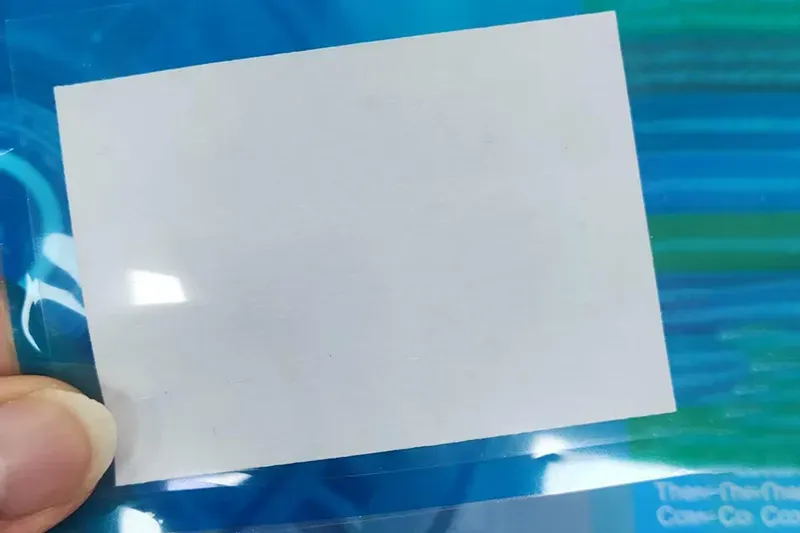
Match pad thickness to the real gap.
- Account for tolerance stacking between parts.
- Set the compression ratio for reliable gap filling.
Controlled deformation preserves mechanical compliance without putting excessive force on optical components.
Boron Nitride Thermal Pads for Optical Module applications work best when compression is snug, not overdone.
Achieving high dielectric breakdown and volume resistivity
• Electrical protection: High dielectric strength, volume resistivity, and insulation resistance limit unwanted current flow.
• Heat plus safety: Strong dielectric breakdown performance supports electrical insulation and voltage endurance near conductive housings.
RoHS compliance, quality certification, and storage condition
Procurement checks should confirm RoHS compliance and suitable quality certification.
- Follow the stated regulatory standard and environmental safety requirements.
- Respect the recommended storage condition and shelf life before assembly.
For Boron Nitride Thermal Pads for Optical Module production, Sheen Technology can align material documentation with purchasing and manufacturing needs.
How Do BN Thermal Pads Work?
Boron Nitride Thermal Pads for Optical Module designs move heat away from compact electronics without creating an electrical path. In practice, the soft composite fills tiny surface gaps, so heat can reach a housing or heat spreader with less trouble. This makes BN thermal pads useful where tight space and steady heat management meet.
Polymer matrix dispersion of ceramic filler for heat flow
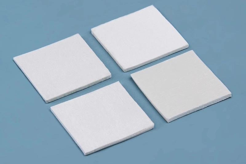
Inside Boron Nitride Thermal Pads for Optical Module applications:
- Boron Nitride acts as the ceramic filler inside a flexible polymer matrix.
- Even particle dispersion helps build continuous paths for heat flow, improving thermal conductivity.
The resulting composite material stays electrically insulating while fitting around delicate parts.
Heat dissipation pathways through reduced thermal resistance
A BN thermal pad helps heat dissipation by creating a shorter thermal pathway toward the housing.
At the interface:
- Soft contact fills air pockets, cutting thermal resistance.
- Better thermal transfer supports cooling while electrical insulation remains intact.
Within the filler:
- Good particle contact can limit disruptive phonon scattering, helping heat move along efficiently.
Die-cut dimension and surface area’s role in contact efficiency
Accurate die-cut geometry sounds simple, but it matters a lot.
Fit and coverage
- Correct dimension places the pad over the intended hot spot.
- Adequate surface area increases thermal contact.
Mechanical fit
- Balanced interface pressure supports contact efficiency without stressing optical parts.
- Suitable geometry avoids wasted material or poor coverage.
Operating temperature range in optical module environments
Boron Nitride Thermal Pads for Optical Module assemblies face steady heating and repeated cycling.
During operation:
- A suitable operating temperature and temperature range preserve thermal stability.
- Consistent behavior supports heat management inside each optical module.
- Stable properties across the working environment help maintain long-term reliability.
3 Advantages Of Thermal Pads In Optical Modules
Boron Nitride Thermal Pads for Optical Module applications tackle heat, insulation, and tricky assembly gaps in one go. These practical advantages help compact optical hardware operate reliably while keeping production straightforward.
Improved heat dissipation for laser diode longevity
Heat control starts at the source. Boron Nitride pads create a low-resistance path from the laser diode toward the housing.
- Higher thermal conductivity supports steady heat dissipation, helping limit junction temperature during continuous data transmission.
- Better thermal management can reduce heat-driven aging and support a longer operational lifespan.
Sheen Technology Boron Nitride Thermal Pads for Optical Module designs provide practical thermal contact where space is tight, so excess heat has somewhere useful to go.
Electrical insulation safeguarding optoelectronic devices
Boron Nitride Thermal Pads for Optical Module designs do more than move heat. Their electrical insulation and high dielectric strength isolate optoelectronic devices from conductive metal surfaces.
- That separation supports short-circuit protection without adding a bulky barrier.
- Strong resistance to voltage breakdown also helps preserve signal integrity in densely packed optical hardware.
In short, BN thermal pads combine electrical isolation and heat transfer in one interface.
Streamlined installation in transceiver housing designs
Easier fitting comes from material adaptability. A BN thermal interface material works as a conformable gap filler.
- Mechanical flexibility accommodates small height variations.
- Controlled compression improves contact inside a compact design.
- Pre-cut shapes simplify the assembly process,No liquid compound means less mess around the transceiver housing.
Sheen Technology supplies Boron Nitride Thermal Pads for Optical Module integration where repeatable placement matters, making optical module assembly quicker and easier to manage.
Ceramic Vs. Boron Nitride Thermal Pads
Picking a pad is not just about chasing the biggest conductivity number. Ceramic and BN compounds balance heat flow, insulation, thickness, and price differently. For optical hardware, Boron Nitride Thermal Pads for Optical Module designs can move heat while keeping circuits isolated. Sheen Technology offers both material routes, helping engineers match a thermal interface to real operating conditions without overcomplicating the job.
Ceramic filler pads
Ceramic pads commonly use alumina filler dispersed through silicone. They are a cost-effective choice when useful thermal conductivity and dependable electrical insulation matter.
Thermal behavior
- More filler can improve heat dissipation.
- Thinner pads generally reduce thermal resistance, though compression still matters.
Electrical behavior
- High dielectric strength helps separate powered parts from a metal housing.
- For less demanding optical module builds, these pads can keep cost in check.
For quick comparison, typical engineering ranges—not guaranteed product specifications—show why material grade matters:
| Filler system | Conductivity (W/m·K) | Typical thickness (mm) |
| Alumina silicone | 1.0–2.0 | 0.5–5.0 |
| Alumina silicone | 2.0–3.0 | 0.5–3.0 |
| Alumina-rich | 3.0–5.0 | 0.5–2.0 |
| Sheen Technology BN Thermal pad | 16.0 | 0.2–5.0 |
*Typical engineering ranges for each filler class, not guaranteed product specifications. Grades vary; datasheets govern.
Boron nitride thermal pads
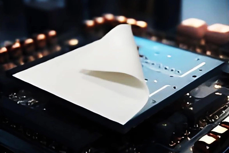
Hexagonal boron nitride offers high thermal conductivity alongside strong electrical isolation. That combo is a handy fit for Boron Nitride Thermal Pads for Optical Module applications where compact electronics generate concentrated heat.
- A BN thermal interface material fills small air gaps between an optical module and heat sink.
- Its low dielectric constant supports electrically sensitive designs, while good temperature stability helps under changing loads.
- Boron Nitride Thermal Pads for Optical Module builds can therefore favor heat transfer without giving up insulation.
For higher heat-flux hardware, Sheen Technology can match BN pad thickness and hardness to contact pressure. Boron Nitride Thermal Pads for Optical Module designs, also called BN thermal pads, are especially useful when electrical separation and steady cooling have to work together.
Data Center Optics: Cooling Challenges
Compact optical hardware puts a lot of heat into very little space, so good cooling is a big deal. Boron Nitride Thermal Pads for Optical Module designs can move heat while providing insulation. Choosing the right thermal pad also depends on contact geometry, compression, and storage before assembly.
High-density fiber optic communication heat buildup
As transceiver density rises:
- Faster fiber optic communication increases local heat flux.
- Compact optical module layouts leave less room for heat dissipation.
Boron Nitride Thermal Pads for Optical Module assemblies support thermal management by carrying heat toward the housing.
Better temperature control helps prevent hot components from throttling or drifting.
Maintaining sufficient surface area for heat spread
A larger surface area gives an interface material more room to pass heat into the heat spreader. That sounds simple, but uneven parts can spoil the deal by increasing contact resistance.
| Pad contact area | Conductivity | Relative contact area |
| 100 mm² | 3 W/m·K | 25% |
| 200 mm² | 3 W/m·K | 50% |
| 300 mm² | 3 W/m·K | 75% |
| 400 mm² | 3 W/m·K | 100% |
Good geometric design and thermal conductivity improve cooling efficiency.
Lowering thermal resistance in modular transceivers
Fit the Boron Nitride Thermal Pads for Optical Module solution to the available gap.
- Limit excess thickness, which raises thermal resistance.
- Apply enough compression for reliable heat transfer.
Check material properties.
- Boron nitride supports electrical insulation.
- A conformable thermal pad reduces interface impedance around a modular transceiver.
Impact of shelf life and storage conditions on performance
Shelf life matters. Poor storage condition can accelerate polymer aging and material degradation, so:
- Environmental stability — control heat and humidity.
- Thermal stability — follow supplier temperature limits.
- Reliability — keep packaging sealed until use.
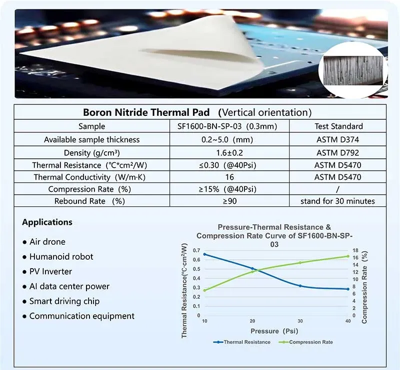
Stored correctly, boron nitride thermal pads retain flexibility and compression more consistently before installation. As stated in the Sheen Technology boron nitride Thermal pad datasheet, it has a compression rate of >15% (at 40 psi) and a rebound rate of >90%.
Overheating Modules? Try BN Thermal Pads
Heat packed inside compact optics can quickly become a headache. Boron Nitride Thermal Pads for Optical Module applications combine heat transfer, cushioning, and electrical isolation, helping sensitive parts stay cooler. Sheen Technology offers Boron Nitride thermal pad options designed for demanding optical module assembly.
Boosting Shore hardness and tensile strength for durability
For Boron Nitride Thermal Pads for Optical Module designs, mechanical properties affect both fit and service life.
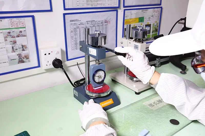
Assembly performance
- Shore hardness balances firmness with conformability around uneven parts.
- Tensile strength and tear resistance help prevent damage during placement.
Long-term reliability
- Controlled elongation lets the polymer matrix flex under pressure.
- Good mechanical stability supports repeated thermal cycling and overall mechanical durability.
That balance matters when tight assembly tolerances leave little room for error.
Enhancing electrical insulation with stable dielectric constant
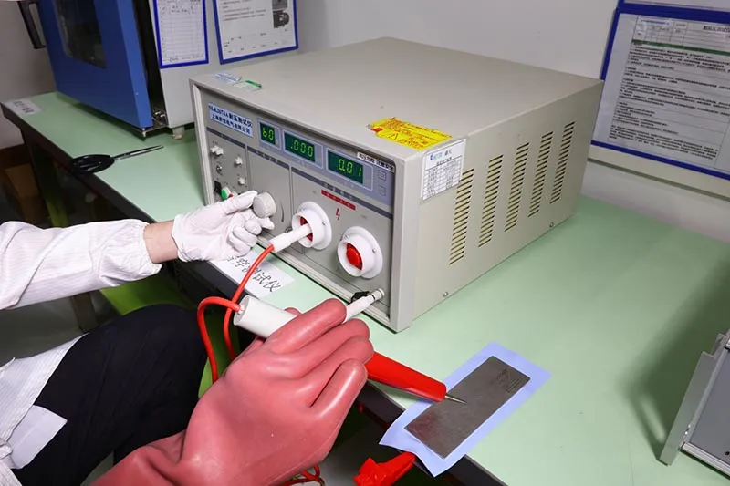
BN thermal pads need to move heat without creating an electrical path. Stable electrical insulation starts with a controlled dielectric constant, while high volume resistivity supports dependable insulation resistance.
- Check dielectric strength against the operating voltage.
- Review dissipation factor for electrical loss.
- Confirm the rated voltage breakdown margin.
This mix makes Boron Nitride thermal interface pads practical near sensitive optoelectronic circuitry.
Verifying the material safety data sheet for procurement peace of mind
Procurement gets a clearer paper trail by checking the Material Safety Data Sheet before ordering.
Documentation checks
- Review the MSDS for hazard identification and chemical composition.
- Confirm storage, handling, and toxicological data.
Approval checks
- Match compliance records with applicable regulatory standards.
- Verify RoHS documentation and environmental safety claims.
It is a simple check, but it can save a lot of back-and-forth during supplier approval.
Sheen Technology manufactures BN pads alongside vertically aligned graphene, carbon fiber and graphite constructions, with die-cutting, film lamination and edge sealing, and can review module drawings to recommend which interface belongs at which location.
Request BN Pad Samples with Test Reports →
Internal Linking:
- Boron Nitride Thermal Pad for AI Servers: Is It Better Than Alumina
- Boron Nitride Thermal Pad vs. Thermal Grease for Inverter Power Modules
- Vertically Aligned Graphene Thermal Pad vs. Silicone: Which Wins
- How to Select a Thermal Pad for OSFP and QSFP-DD Optical Modules
- Thermal Management for 1.6T Optical Transceivers: Key Design Challenges
Sheen Thermal
Dongguan Sheen Electronic Technology Co., Ltd · Founded in 2008
Manufacturer of thermal interface materials and silicone foam for automotive electronics, energy storage, power electronics, communications and consumer electronics.
Certified
- ISO 9001:2015
- ISO 14001:2015
- IATF 16949:2016
What we supply
- Thermal conductivity Up to 90 W/m·K
- Thickness 0.3–10.0 mm
- Custom & samples Die-cut to drawing, 3–7 days