
 English
 usheenthermal

Riding Heat Sink vs Drop-Down Heat Sink for High-Power Optical Modules
Date:2026-09-04
High-Power Optical Modules run hot, so riding versus drop-down heat sinks isn’t small potatoes. Riding designs favor top-side cooling; drop-down designs move heat around or below the assembly.
That choice shapes material sourcing too—from thermal interface material to copper tungsten heatsinks, AlN baseplates, and thermoelectric coolers.
Sheen Technology manufactures thermal interface materials — boron nitride insulating pads, vertically aligned graphene and carbon fiber pads, phase-change materials, gap fillers and thermally conductive epoxies — and supports material-to-package matching against customer drawings. Heat sink and baseplate geometry remain the module designer’s decision; this article addresses the interface layer each architecture requires.
Request the Optical Module Interface Material Guide →
Reading Notes for High-Power Optical Modules
➔ Sink Selection: Riding sinks excel at top‐side cooling without PCB interference, while drop‐down sinks route heat below constrained packages.
➔ Substrate Matching: Indium phosphide lasers need low thermal resistance mounts, GaAs wafers favor CuW heatsinks, and silicon photonics demand alignment-friendly baseplates.
➔ Material Synergy: Combine thermal interface materials, graphite sheets, or phase-change layers with epoxies and underfills to minimize contact resistance and mechanical stress.
➔ Deployment Context: In dense racks, riding sinks preserve RF clearance and flex-circuit routing; drop-downs pair well with TECs and dielectric insulation for wavelength stability.
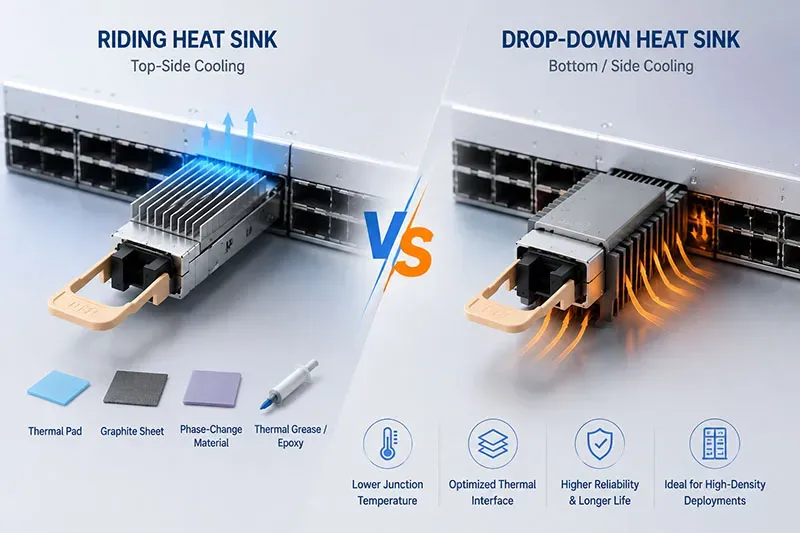
This image is a conceptual illustration and does not represent the actual appearance, size, or internal structure of the product.
Riding Vs Drop-Down Sinks Overview
High-Power Optical Modules pack serious heat into tight hardware, so sink geometry can make or break stable operation. Riding and drop-down designs move heat differently while keeping optical links practical to assemble and service. For High-Power Optical Modules, engineers also need to balance airflow, PCB space, contact pressure, and cooling capacity without making the package bulky or tricky to maintain.
Riding heat sink
A riding sink sits on the module housing, using thermal interface material to bridge tiny surface gaps. That simple setup suits many high-power optical systems and keeps PCB space relatively open.
Contact and fit
- Surface mounting keeps installation straightforward.
- A lower thermal resistance helps High-Power Optical Modules shed concentrated heat.
Cooling behavior
- Convective cooling carries heat from fins into moving air.
- A controlled height profile can preserve chassis clearance without going overboard.
Sheen Technology supplies the interface layer — die-cut to the housing footprint, with controlled thickness and hardness selected against the available cage clamping force — and can review drawings to propose a candidate stack. Heat sink geometry itself is specified by the module or system designer.
Drop-down heat sink
Drop-down designs reach beside or below optical modules, making them handy when top-side room is tight.
Mechanical path
- A PCB cutout provides room for the lowered structure.
- Adequate mechanical clearance reduces interference with nearby parts.
Thermal path
- Direct contact can move heat toward a baseplate, supporting stronger thermal dissipation.
- An integrated fin arrangement can work with targeted airflow management.
Riding vs. drop-down: architecture decision matrix:
| Constraint | Riding Sink | Drop-Down Sink |
| Top-side height available | Required — consumes cage headroom | Not required — clears the top face |
| PCB area around module | Preserved — no cutout | Consumed — cutout removes routing layers |
| RF / flex routing clearance | Good — side space stays open | Reduced — pedestal and cutout intrude |
| Conduction path length | Short (housing top → sink base) | Can be shorter to a bottom hot zone, longer to a remote baseplate |
| Contact area | Large (full housing top face) | Small and defined (pedestal footprint) |
| Available contact pressure | Low — limited by cage retention | Higher — set by pedestal standoff design |
| Interface material bias | Soft pad, PCM or grease at low pressure | Thickness-controlled pad or PCM; squeeze-out must be controlled |
| Pairs well with | Graphite spreading film on the housing | TEC, dielectric isolation layer, baseplate |
| Main risk | Insufficient convective capacity at low airflow | Cutout routing loss and pedestal coplanarity error |
Send Us Your Module Drawing for Interface Material Matching →
Which Sink Suits High-Power Modules?
High-Power Optical Modules pack substantial heat into tight spaces, so sink geometry matters as much as material choice. Good thermal paths protect optical power, wavelength stability, and service life. For high-power modules, the practical goal is pretty simple: move heat fast without upsetting alignment.
Matching Indium Phosphide substrate modules to sink type
Indium Phosphide lasers create concentrated heat, giving High-Power Optical Modules demanding thermal dissipation needs.
Match the optical module around its mechanical layout:
- Choose a riding heat sink when top clearance and contact pressure are predictable.
- Use a drop-down heat sink when substrate integration places the hot zone below the surrounding frame.
- Check high-power density against junction limits. Lower interface resistance generally keeps laser temperature steadier.
Gallium Arsenide wafer assemblies: sink compatibility
For High-Power Optical Modules using Gallium Arsenide, flat support helps prevent local hot spots.
Start with the wafer assembly and expected junction temperature.
- Compare thermal resistance and cooling performance using measured package data.
- Check sink compatibility with the optoelectronic device footprint.
| Material | In-plane (W/m·K)* | Through-plane (W/m·K)* | CTE (10⁻⁶/K)* | Electrically |
| Copper | 400 (isotropic) | 400 (isotropic) | 17 | Conductive |
| Aluminium | 205 (isotropic) | 205 (isotropic) | 23 | Conductive |
| CuW (tungsten copper) | ~200 (isotropic) | ~200 (isotropic) | 6–8 (tunable) | Conductive |
| AlN (aluminium nitride) | ~170 (isotropic) | ~170 (isotropic) | ~4.5 | Insulating |
| Graphite sheet | 300–1,500 | 5–20 | ~1 (in-plane) | Conductive |
| Vertically aligned graphene pad | — (pad form) | 75-90 | Matrix-dependent | Conductive |
| Boron nitride pad | — (pad form) | 16 | Matrix-dependent | Insulating |
*Publicly published typical values for each material class; not measured Sheen product data and not a performance promise. Grades vary by supplier and processing; datasheets govern.
Silicon Photonics chip integration with heat sinks
Silicon Photonics adds optical alignment and connector clearance to thermal management.
For High-Power Optical Modules:
- A riding heat sink can simplify top-side heat dissipation.
- A drop-down heat sink can fit carrier-based chip integration.
- Keep the optical transceiver path clear for fibers and high-speed connectors.
For high-power optical assemblies, Sheen Technology can match sink geometry to package drawings rather than forcing a one-size-fits-all fit.
How Riding Heat Sinks Can Supercharge High-Power Optical Module Performance
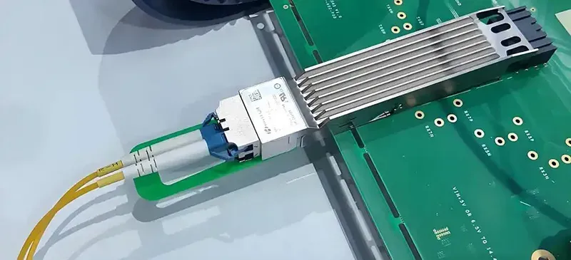
High-Power Optical Modules pack serious heat into tight spaces. Smart riding-sink design keeps that heat moving, helping Sheen Technology build optical module hardware that stays cooler, steadier, and ready for demanding optical links.
Enhancing laser diode chip cooling with copper tungsten heatsink
A laser diode chip creates a concentrated hot spot during high-power operation. Copper tungsten gives the heatsink a useful mix of strong heat dissipation and controlled expansion, so the ceramic submount sees less mechanical strain.
For High-Power Optical Modules, that makes thermal management a big deal: heat spreads away from the chip instead of hanging around.
Epoxy adhesive and thermal interface material for optimal heat transfer
Getting heat across mating surfaces sounds simple, but tiny air gaps can throw a wrench in the works.
- Epoxy adhesive keeps the riding sink mechanically secure.
- Thermal interface material fills microscopic gaps, improving thermal conductivity and heat transfer.
- Lower interface resistance helps High-Power Optical Modules move heat toward the sink.
- Better thermal management also keeps the optical module package mechanically stable.
Gold bonding wire and high-speed connector reliability at elevated temperatures
Cooling also protects electrical paths inside High-Power Optical Modules.
- Reduced elevated temperature limits repeated thermal stress.
- Lower stress can slow fatigue in gold bonding wire.
- Cooler operation supports high-speed connector reliability, preserving signal integrity as optical power rises.
For Sheen Technology, effective riding-sink cooling therefore supports both thermal control and dependable high-power optical module performance.
4 Benefits Of Drop-Down Heat Sinks
High-Power Optical Modules pack lasers, detectors, and control electronics into tight spaces, so heat can become a headache fast. A drop-down layout creates a shorter path from hot optical parts to the cooling surface. For High-Power Optical Modules, Sheen Technology thermal designs can combine insulation, interface materials, heat spreading, and active cooling to support steady operation.
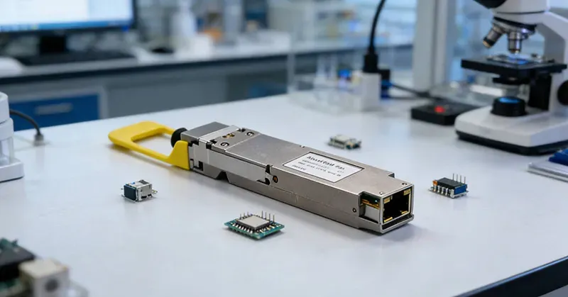
Superior dielectric material insulation against thermal cycling
A drop-down heat sink can sit close to insulated conductors without compromising electrical insulation.
Thermal protection
- Dielectric material separates electrically active features.
- During thermal cycling, controlled heat flow can reduce thermal stress caused by expansion differences, supporting long-term reliability.
Underfill material synergy for photodetector array stability
A photodetector array needs tiny connections to stay put as temperatures change.
Package support
- Underfill material distributes stress around solder joints.
- Lower thermal expansion strain can improve joint reliability.
In High-Power Optical Modules, nearby cooling aids mechanical stability within compact optical modules.
Graphite thermal sheet improving modulator component lifespan
A graphite thermal sheet offers high in-plane thermal conductivity, moving concentrated heat from a modulator component toward the sink. That extra heat dissipation matters in high-power optics, where persistent hotspots can alter optical behavior and shorten component lifespan.
| Design target | Typical evaluation point | Value |
| Interface temperature | operating target | 60 °C |
| Temperature swing | cycling example | 80 °C |
| Graphite thickness | design example | 0.10 mm |
*Values are representative engineering evaluation points, not universal component ratings.
Two constraints are non-negotiable.
- Direction: graphite film spreads laterally and is a poor through-plane conductor at roughly 5–20 W/m·K. A graphite film used as the only layer between a hot die and a sink makes the joint worse, not better.
- Electricity: graphite is conductive. In an optical module the spreading path commonly runs over RF transmission lines, gold bond wires, exposed pads and high-speed connector leads. Specify edge sealing or polyimide film lamination, verify dielectric strength to ASTM D149 / IEC 60243, and confirm creepage and clearance to the nearest live feature before release.
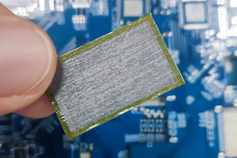
Sheen Technology’s graphene thermal pads are optimized based on these two constraints, utilizing a vertically aligned structure and incorporating edge sealing.
Thermoelectric cooler pairing for optical multiplexer efficiency
Pairing a thermoelectric cooler with the sink gives High-Power Optical Modules tighter temperature control.
Optical side
- An optical multiplexer benefits from stable wavelength alignment.
Cooling side
- Better thermal management improves heat rejection and cooling performance.
- Keeping the cooler near its intended operating point can also support energy efficiency.
Data-Center: Riding Sinks For Dense Racks
Dense racks make every millimeter count. Riding sinks move cooling above High-Power Optical Modules, leaving valuable side space for RF traces, flex circuits, and passive parts. This setup helps optical hardware stay cooler without boxing in designers who still need clean electrical paths and practical assembly access.
RF transmission line clearance in tight rack layouts
For High-Power Optical Modules, top-side cooling keeps the RF transmission line path open.
RF path
- Added high-frequency clearance makes circuit routing less cramped.
- Stable spacing supports impedance matching and signal integrity.
- Shorter detours can also limit electromagnetic interference in a dense rack layout.
That’s a handy win for high-power optical hardware where tiny layout changes matter.
Flexible printed circuit routing around aluminum nitride baseplate
A flexible printed circuit often needs a gentle path beside an aluminum nitride baseplate.
Thermal path
- High thermal conductivity spreads heat from High-Power Optical Modules.
Routing path
- Side clearance gives circuit routing room around the substrate.
- Smoother bends reduce mechanical stress.
The result is compact high-power module packaging without forcing the flex into a tight corner.
EMI suppression filter and multilayer ceramic capacitor resilience
Lower temperatures help passive parts near High-Power Optical Modules handle daily thermal cycling.
Power-conditioning parts
- An EMI suppression filter supports electromagnetic compatibility.
- Reduced thermal stress can aid long-term component resilience.
- A multilayer ceramic capacitor benefits from gentler temperature swings.
- Better thermal control supports each passive component used for circuit protection.
For high-power optical modules, that cooler neighborhood can mean steadier power behavior over time.
Riding and drop-down heat sinks solve different geometric problems, and the architecture chosen determines which interface material can work at all. Riding sinks preserve board area and RF clearance but operate at low contact pressure and are capped by cage headroom and airflow; drop-down sinks clear the top face and can shorten the path to a bottom hot zone, at the cost of PCB routing area and tighter coplanarity control.
Contact Sheen Technology for Package-to-Material Matching →
Internal Linking:
- How to Select a Thermal Pad for OSFP and QSFP-DD Optical Modules
- Thermal Management Solutions for Optical Modules in High-Mating-Cycle Scenarios
- Testing the Graphene Thermal Pad for 800G OSFP Module Reliability
- Vertically Aligned Graphene Thermal Pad vs. Silicone
- How to Test Graphene TIMs Under ASTM D5470
Sheen Thermal
Dongguan Sheen Electronic Technology Co., Ltd · Founded in 2008
Manufacturer of thermal interface materials and silicone foam for automotive electronics, energy storage, power electronics, communications and consumer electronics.
Certified
- ISO 9001:2015
- ISO 14001:2015
- IATF 16949:2016
What we supply
- Thermal conductivity Up to 90 W/m·K
- Thickness 0.3–10.0 mm
- Custom & samples Die-cut to drawing, 3–7 days