
 English
 usheenthermal

800G to 1.6T: What Changes in Optical Module Thermal Design?
Date:2026-09-04
With the increasing power consumption of 800G and 1.6T optical modules, the heat generated by the chips and devices needs to be transferred to the housing or heatsink through a short but critical interface.
Optical Module Thermal Design gets trickier at 1.6T: tighter packages can turn DSP and optical-engine hotspots into a serious sourcing headache. More bandwidth doesn’t automatically mean twice the heat, but heat density and interface resistance matter more.
Sheen Technology engineers advise evaluating thermal materials by interface resistance, bond-line control, reliability, and manufacturability—not conductivity alone. This guide shows what changes.
Request the 1.6T Optical Module Interface Material Guide →
Harmonic Highlights: Optical Module Thermal Design
➔ Speed vs. Heat: Evaluate pad conductivity and vapor-chamber spread as data rates double from 800G to 1.6T; focus on interface resistance and hotspot density rather than raw power.
➔ Material Match: Select substrates (AlN, CuW) and TIMs (phase-change, graphite) by thermal conductivity, bond-line control, and reworkability to balance heat paths and mechanical stresses.
➔ Validation Loop: Integrate heat-flux sensors, IR imaging, and thermal resistance fixtures under realistic traffic and airflow to verify designs and ensure long-term reliability.
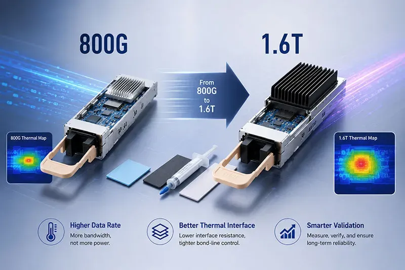
Note: This diagram was created with the assistance of AI and is not an actual photograph; the structure and logic shown are for reference only.
What Actually Changes from 800G to 1.6T
Moving from 800G to 1.6T pushes electrical power and heat into nearly the same footprint.
The useful way to read the transition is to separate three quantities that are often conflated: total module power, power per bit, and local heat flux. All three move, but not in the same direction, and only two of them create thermal difficulty.
Power Rises, Power-per-Bit Falls
More bandwidth doesn’t automatically mean twice the heat.
A generation of DSP process scaling and the move to higher-order modulation means 1.6T modules carry roughly double the traffic without doubling dissipation. Published industry figures put typical 800G pluggable modules in the mid-to-high teens of watts, and 1.6T pluggable modules meaningfully higher — but the increase is well short of proportional, and it varies by reach, form factor and whether the design uses linear drive or a full DSP. Treat these as industry-level ranges for budgeting, not as datasheet values for any specific module.
The consequence for thermal design is that the module-level power number understates the difficulty. What governs junction and case temperature is the flux under the DSP die and the resistance of the path out to the housing — and both of those worsen even when total power looks manageable.
The Enclosure Does Not Grow
Pluggable module external dimensions are fixed by multi-source agreement, and the cage that surrounds them fixes the available heatsink volume. Higher dissipation therefore has to leave through substantially the same external surface area as before. Since convective capacity is set by that surface and the system air path, the only remaining lever is how little resistance the conduction path offers between the hot die and the housing.
| Parameter | Direction | Consequence for Interface Design |
| Module power dissipation | Rises, sub-proportionally | Higher total load through the same housing area |
| Power per bit | Falls | Do not scale the thermal budget linearly with data rate |
| DSP local heat flux | Rises | Spreading becomes necessary; a single bulk path is no longer sufficient |
| Available heatsink volume | Fixed by the cage | Convective capacity is capped; conduction resistance is the controllable variable |
| Tolerance for bond-line thickness | Tightens | Thickness-controlled pads, films or PCM replace free-dispensed gels |
| Sensitivity to coplanarity error | Rises | Compressible, vertically aligned pads over rigid constructions |
| Cycling severity | Rises with duty and delta-T | Screen pump-out, compression set and dry-out before release |
*Directional summary of the industry transition. Magnitudes depend on form factor, reach and architecture; this table describes what to re-examine, not measured results.
Interface Materials at Higher Power Density
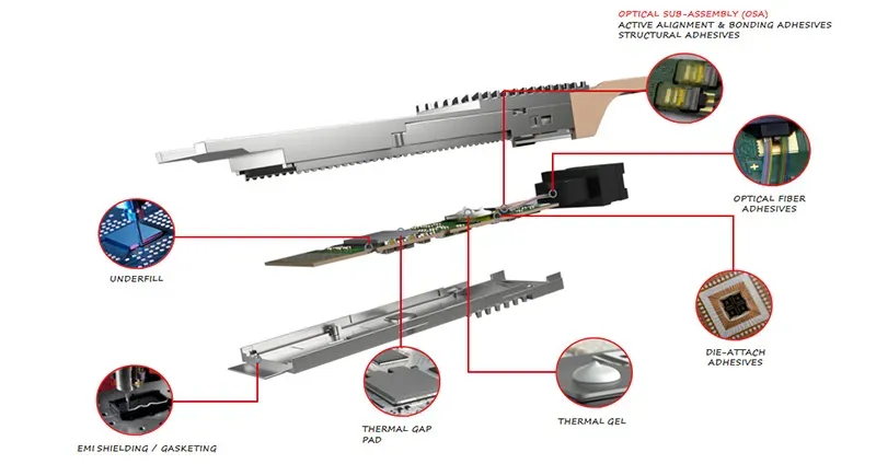
Thermal Pads and Gels Across the Rate Transition
A thermal pad looks simple, but rising data rate can expose small contact problems fast.
- Thermal conductivity controls heat movement through the material.
- Compression rate affects contact with uneven DSP and housing surfaces.
- Excess thickness increases thermal resistance.
- while weak pressure can leave tiny air gaps.
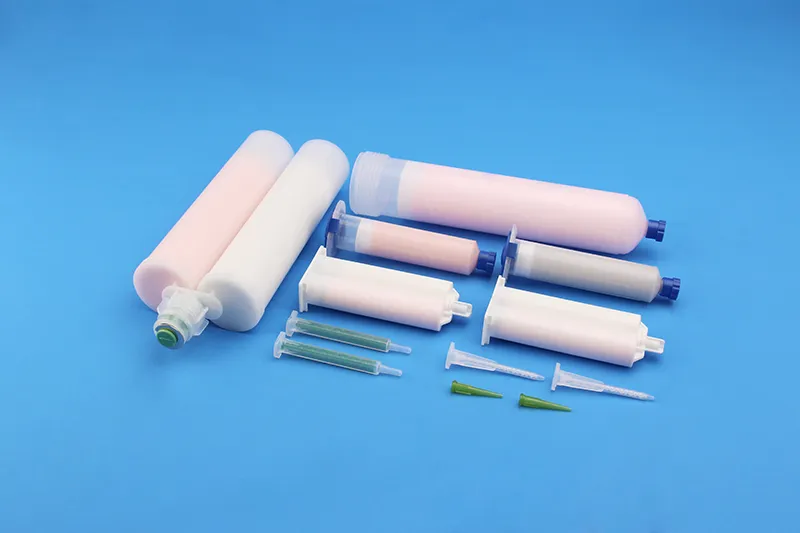
In this context, applying thermal conductive gel via dispensing offers better adaptability to height variations, complex gaps, and automated production setups. The SE120 features a thermal conductivity of 12 W/(m·K) and a bond line thickness (BLT) of less than 0.2 mm, making it suitable for automated dispensing processes in a semi-flowable state. It cures in under 2 hours at 85°C and offers a working time of at least 48 hours at 25°C.
At 1.6T the same gel becomes a liability, precisely because its bond line is set by dispense volume and clamp force rather than by a controlled dimension. Module-to-module variation in bond-line thickness translates directly into variation in case temperature, and that variation is what consumes the thermal margin.
The move at 1.6T is therefore toward thickness-controlled constructions — die-cut pads, phase-change films, or gels applied under a defined compression stop. Sheen Technology can evaluate these contact conditions alongside mechanical tolerances, helping balance pad softness, pressure, and practical assembly limits.
Phase-Change Material
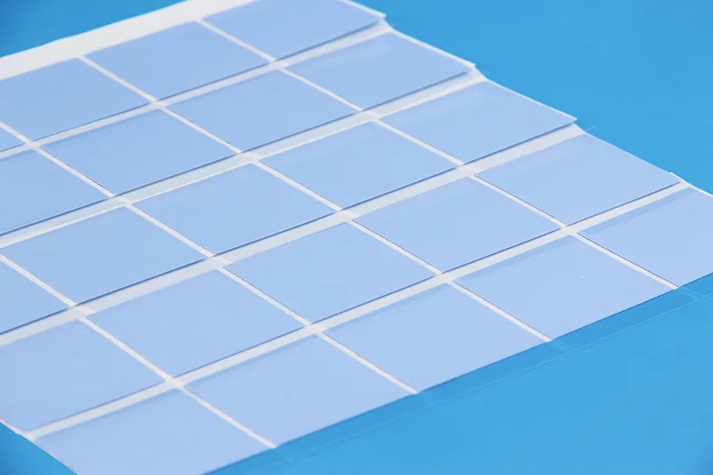
A phase change material softens near its working temperature, improving compliance and lowering thermal resistance with a thin bond line.
Above its transition the material flows under mounting pressure, wets both surfaces and expels trapped air, reaching a bond line typically in the 0.025–0.10 mm range for server- and telecom-grade films. The resistance drop comes from wetting and thickness reduction, not from latent-heat absorption, which is negligible against the steady heat flow the interface carries.
Graphite Spreading Film
Graphite sheet provides strong in-plane thermal conductivity, making it handy for moving hotspot heat sideways.
A graphite spreading film is the correct choice when the problem is a concentrated DSP or optical-engine hotspot that must be distributed over a wider area before it enters the housing. In-plane conductivity of roughly 300 to 1,500 W/m·K does that in a film typically 25 to 100 µm thick — a fraction of the height an equivalent metal spreader would consume, and a fraction of the mass.
Vertically Aligned Graphene Pad
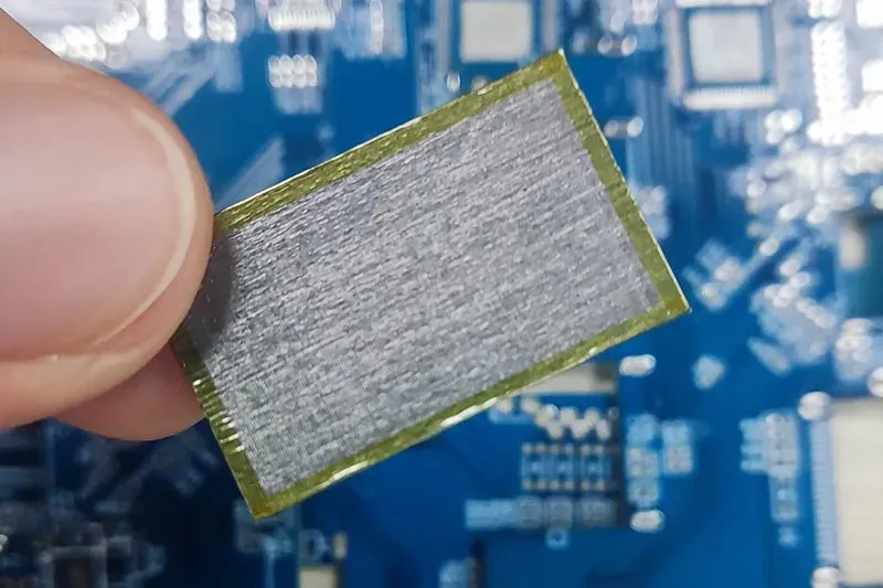
Where heat must cross the bond line rather than spread along it, a vertically aligned graphene pad is the carbon-based answer.
Taking GSF90-03 as an example, its standard thickness is 0.3±10%, its thermal resistance is no higher than 0.10℃·cm²/W under 40psi conditions, its compression ratio is no less than 30%, and its operating temperature range is -40~150℃. Typical applications include high-power modules such as optical modules.
This type of material is suitable for structures where interfacial thermal resistance and material thickness are important, but assembly conditions must also be considered. Contact area, interface flatness, and the ability to provide sufficient pressure during assembly all affect the final bonding state.
If the structure itself cannot provide sufficient pressure, the material performance may not be fully realized; if the pressure is too high, the device and PCB must be assessed for their ability to withstand it.
Graphene is electrically conductive. Specify edge sealing or film lamination wherever the pad is adjacent to live features, and confirm the isolation scheme during qualification rather than after it.
Boron Nitride Insulating Pad
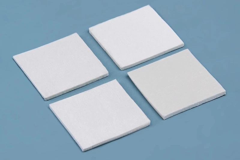
Where the interface must carry heat and block current, a boron nitride filled pad is the reference choice. Hexagonal boron nitride combines useful through-plane conductivity with high dielectric strength and a low dielectric constant, so it can be placed directly over DSP power rails and high-speed routing without a separate isolation layer — which removes a layer from the stack, and a removed layer is a removed thermal resistance.
| Material | Strong Direction | Electrically | Thickness Control | Best Fit at 1.6T |
| Thermal gel | Through-plane | Depends on filler | Poor — set by dispense volume | 800G; tolerance-tolerant, variable bond line |
| Die-cut gap pad | Through-plane | Depends on filler | Good — specified dimension | Height variation across components |
| Phase-change film | Through-plane | Depends on filler | Good — thinnest bond line | Flat clamped interfaces, lowest resistance |
| Vertically aligned graphene pad | Through-plane | Conductive | Good | High through-plane flux plus coplanarity error |
| Vertically aligned carbon fiber pad | Through-plane | Conductive | Good | Thicker gap, higher clamp force |
| Boron nitride pad | Through-plane | Insulating | Good | Interface above live rails or lanes |
| Graphite spreading film | In-plane | Conductive | Film — 25–100 µm | Lateral spreading only; never the sole interface layer |
| Conductive epoxy | Through-plane | Depends on filler | Cure-dependent | Fixed gap plus mechanical attachment |
*Typical engineering practice for each material class. Not measured Sheen product data and not a performance promise; datasheets and sample testing govern.
Request 1.6T Interface Material Samples →
4 Steps To Optimize Optical Module Thermal Design
Effective Optical Module Thermal Design starts with materials and ends with proof under real operating loads. As 1.6T modules pack more power into tight spaces, substrate choice, interface control, heat spreading, and accurate testing all matter. Here’s a practical path that keeps optical thermal management from getting too hot to handle.
Step 1: Choose the right substrate (Ceramic, AlN, CuW)
Start with the heat source and package limits.
- Ceramic substrate offers electrical insulation and useful Mechanical strength, but modest Thermal conductivity can limit hotspot spreading.
- Aluminum Nitride combines high conductivity with a Coefficient of thermal expansion close to semiconductor materials. Its low Dielectric constant also suits high-speed optical electronics.
- Copper Tungsten handles concentrated heat well and offers controlled expansion, though weight and machining costs rise.
For Sheen Technology Optical Module Thermal Design, material selection should balance heat flow, electrical needs, weight, and manufacturability rather than chasing conductivity alone.
Step 2: Apply advanced TIMs (Phase change material, graphite sheet)
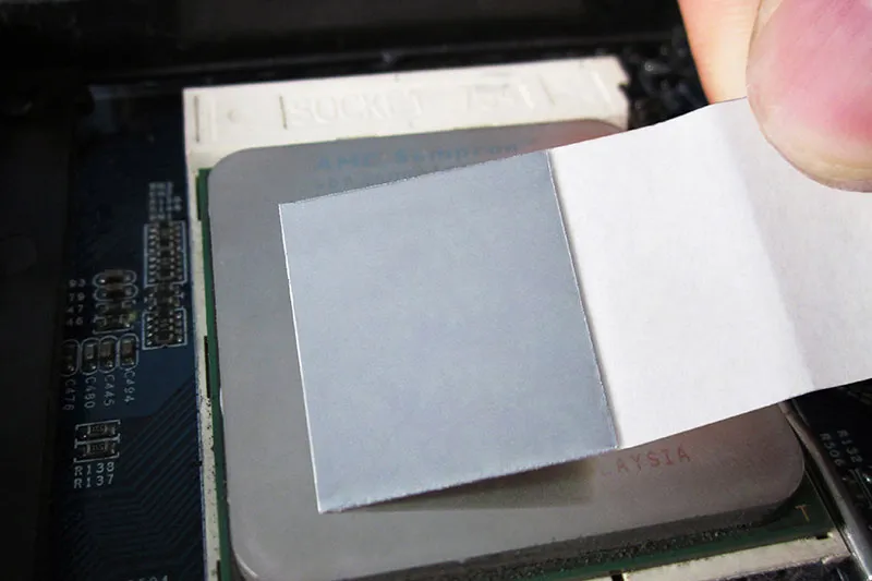
A Thermal interface material closes the tiny Interface gap between hot components and spreaders.
- Phase change material softens near its working temperature, improving Compliance and lowering Thermal resistance with a thin bond line.
- Graphite sheet provides strong in-plane Thermal conductivity, making it handy for moving hotspot heat sideways.
Pressure matters, big time. Check mounting force, spreading direction, rework needs, and resistance at actual 1.6T temperatures.
Step 3: Integrate heat dissipation components (Copper heat sink, vapor chamber)
Match each source to a short thermal path.
- A Copper heat sink provides high conductivity and added Surface area.
- A Vapor chamber spreads dense heat across a wider footprint, using two-phase Fluid dynamics much like a flattened Heat pipe.
Fit cooling to the enclosure.
- Align fins with airflow so Convection can support steady Thermal dissipation.
- Check module volume and neighboring component clearance before locking the design.
Sheen Technology can support this thermal-design approach where rising heat density makes simple metal spreaders less effective.
Step 4: Verify with testing supplies (Infrared thermal imaging film, calibration sample)
Good Optical Module Thermal Design needs measured proof, not guesswork. Use Infrared thermal imaging film for Temperature distribution and Hot spot detection, then compare readings against a traceable Calibration sample.
Add heat-flux sensors and resistance fixtures for repeatable Thermal measurement. Run Thermal testing under realistic traffic, airflow, and ambient temperature; final Validation should confirm stable junction and case temperatures across the intended operating range.
Copper vs. Graphite Film
Optical Module Thermal Design gets tricky when more power is packed into less room. Copper can pull heat directly from hot components, while graphite spreads concentrated heat across a wider area without adding much weight. For 1.6T hardware, good Optical Module Thermal Design often comes down to balancing contact pressure, available space, airflow, and heat-spreading direction without overcomplicating the build.
Copper heat sink
Copper remains a practical choice when Optical Module Thermal Design calls for predictable heat flow in every direction. Its high thermal conductivity lowers the temperature gradient between a hot device and cooler regions, making local heat dissipation easier to control.
Contact and heat flow
A copper metal baseplate provides a rigid, flat mounting surface.
- Good component contact can reduce overall thermal resistance.
- Precise machining supports pockets, fins, screw holes, and custom optical-module shapes.
Dense packaging needs a trade-off.
- Copper's high density adds mass quickly.
- Thick bases and crowded fins may consume volume or restrict airflow.
Sheen Technology can tailor copper parts around component height, contact area, and airflow paths, helping Optical Module Thermal Design stay practical when things get pretty tight inside the module.
Graphite Spreading Film
Graphite sheet changes the thermal strategy. Instead of relying on bulk metal, a thin flexible film uses strong anisotropic conduction to move heat mainly across its surface, supporting lateral heat spreading around concentrated 1.6T hotspots.
The engineering case is specific:
- Where the constraint is lateral transport at low mass and low height, graphite outperforms copper by a wide margin on both.
- Where the constraint is transport through the thickness, it is worse by two orders of magnitude.
The decision is therefore not "copper or graphite" — it is whether the bottleneck in the path is spreading or crossing, and the honest answer in a 1.6T module is usually both, which is why graphite film appears paired with a through-plane pad rather than instead of one.
Overheated Modules? Innovative Thermal Design To Rescue 1.6T
At 1.6T speeds, tiny hot spots can quickly become a big headache. Optical Module Thermal Design has to move heat through tight packages without hurting signal performance or service life. Sheen Technology approaches module thermal design with interface materials, targeted cooling, and practical heat paths that fit the mechanical limits of high-density optical hardware.
Phase change material infusion for hotspot control
A phase change material can soften near its chosen activation temperature, conforming to rough surfaces and reducing interface thermal resistance. That gives a stubborn hotspot a cleaner escape route.
Material selection
- Match melting behavior to normal operating temperatures.
- Check thermal conductivity before assuming softer means better.
Integration
- Control infusion so material stays around the critical interface.
- Add containment to limit pumping or leakage during thermal cycles.
Reliability
- Validate repeated phase changes and long-term heat dissipation.
- Confirm stable temperature control across expected loads.
For Optical Module Thermal Design, that cycling work matters; a quick lab win is no good if interface performance fades later.
Thermoelectric cooler deployment in dense layouts
A thermoelectric cooler uses the Peltier effect to pump heat electrically, making active cooling useful when one device needs tight temperature stabilization.
- Map local heat flux rather than cooling the whole assembly.
- Fit the cooling module into the dense layout with room for electrical connections.
- Carry waste-side heat into the main heat sink; otherwise, the cooler can make the overall thermal problem worse.
Sheen Technology can pair this local temperature-control method with practical optical thermal design, but TEC power draw and condensation limits need careful checking.
Conductive epoxy gap filling to boost interface conductivity
Conductive epoxy works well where mechanical gaps remain fixed after assembly.
Gap control
- Keep gap filling uniform.
- Limit bond-line thickness to reduce thermal resistance.
Material behavior
- Choose a thermal interface material with suitable interface conductivity.
- Match expansion behavior to nearby packages and boards.
Production
- Control curing for dependable bonding.
- Verify the cured path maintains heat transfer after cycling.
Done right, conductive epoxy closes awkward heat paths while adding mechanical attachment, a handy combination when Optical Module thermal design space is seriously tight.
Data Center: Managing 1.6T Module Heat
At 1.6T speeds, heat control gets tricky fast. Optical Module Thermal Design must account for package materials, rack cooling, and solder protection as connected concerns. Good optical module thermal choices keep temperatures steadier under heavy traffic, while practical thermal design limits the wear caused by long data-center duty cycles and repeated heating and cooling.
Liquid crystal polymer packaging for sustained reliability
Optical Module Thermal Design depends heavily on package behavior when modules stay hot for hours.
Material behavior
- Liquid crystal polymer provides a strong Moisture barrier because it absorbs little water, helping limit property changes during long service.
- Its Dimensional stability supports tight package geometry through repeated temperature swings.
Signal and production needs
- Good High-frequency performance helps preserve electrical behavior around fast interfaces.
- Packaging still needs molding and assembly processes that manufacturers can repeat at scale.
The key is Thermal reliability over many cycles, not simply surviving one hot test. That is where optical module packaging earns its keep.
Heat flux sensor monitoring in rack deployments
A Heat flux sensor adds a useful layer to Optical Module Thermal Design because surface temperature alone does not show how much heat is moving.
Place sensors near high-power optics within the Rack deployment.
- Track Real-time data as 1.6T traffic changes.
- Compare heat flow with the local Temperature gradient.
Connect those readings to Thermal monitoring.
- Hotspot changes can expose weak Data center airflow or uneven liquid cooling.
- Traffic-linked readings help teams tell a true load problem from a cooling problem.
That makes rack thermal design easier to tune without guesswork.
Underfill material strategies for long-term stability
Underfill material selection protects fine solder connections in Flip-chip packaging, so it plays a direct role in Optical Module Thermal Design.
Reliability targets
- Match the Coefficient of thermal expansion to nearby materials to reduce Thermal stress.
- Choose thermal conductivity and glass-transition temperature for sustained operating heat.
Assembly targets
- Control flow for complete gap filling and Void prevention.
- Check cure behavior against production limits.
Good matching improves Mechanical reliability and Long-term stability as modules repeatedly heat up and cool down.
The 800G-to-1.6T transition is not a story about twice the heat. It is a story about the same amount of enclosure, more absolute dissipation, higher local flux under the DSP, and a convective capacity the cage fixes before the materials engineer gets involved. That combination moves the decision from the heatsink to the interface.
Sheen Technology manufactures vertically aligned graphene and carbon fiber pads, boron nitride insulating pads, phase-change materials, gap fillers, gels and thermally conductive epoxies, with die-cutting, film lamination and edge sealing, and can review package drawings to propose a candidate stack with datasheet values and test reports.
Contact Sheen Technology for 1.6T Interface Support →
Internal Linking:
- Thermal Management for 1.6T Optical Transceivers: Key Design Challenges
- How Graphene Thermal Pads Optimize 1.6T Optical Transceiver Cooling
- Riding Heat Sink vs. Drop-Down Heat Sink for High-Power Optical Modules
- Vertically Aligned Graphene Thermal Pad vs. Silicone
- How to Test Graphene TIMs Under ASTM D5470
Sheen Thermal
Dongguan Sheen Electronic Technology Co., Ltd · Founded in 2008
Manufacturer of thermal interface materials and silicone foam for automotive electronics, energy storage, power electronics, communications and consumer electronics.
Certified
- ISO 9001:2015
- ISO 14001:2015
- IATF 16949:2016
What we supply
- Thermal conductivity Up to 90 W/m·K
- Thickness 0.3–10.0 mm
- Custom & samples Die-cut to drawing, 3–7 days